Open Nav

The board is then protected by applying a Solder Mask and surface finish (such as Enig or Hasl), while Silkscreen legends are printed for Component Identification. Finally, strict Quality Assurance—including Automated Optical Inspection (Aoi) and Electrical Testing—ensures every board meets exacting industry standards before shipment.
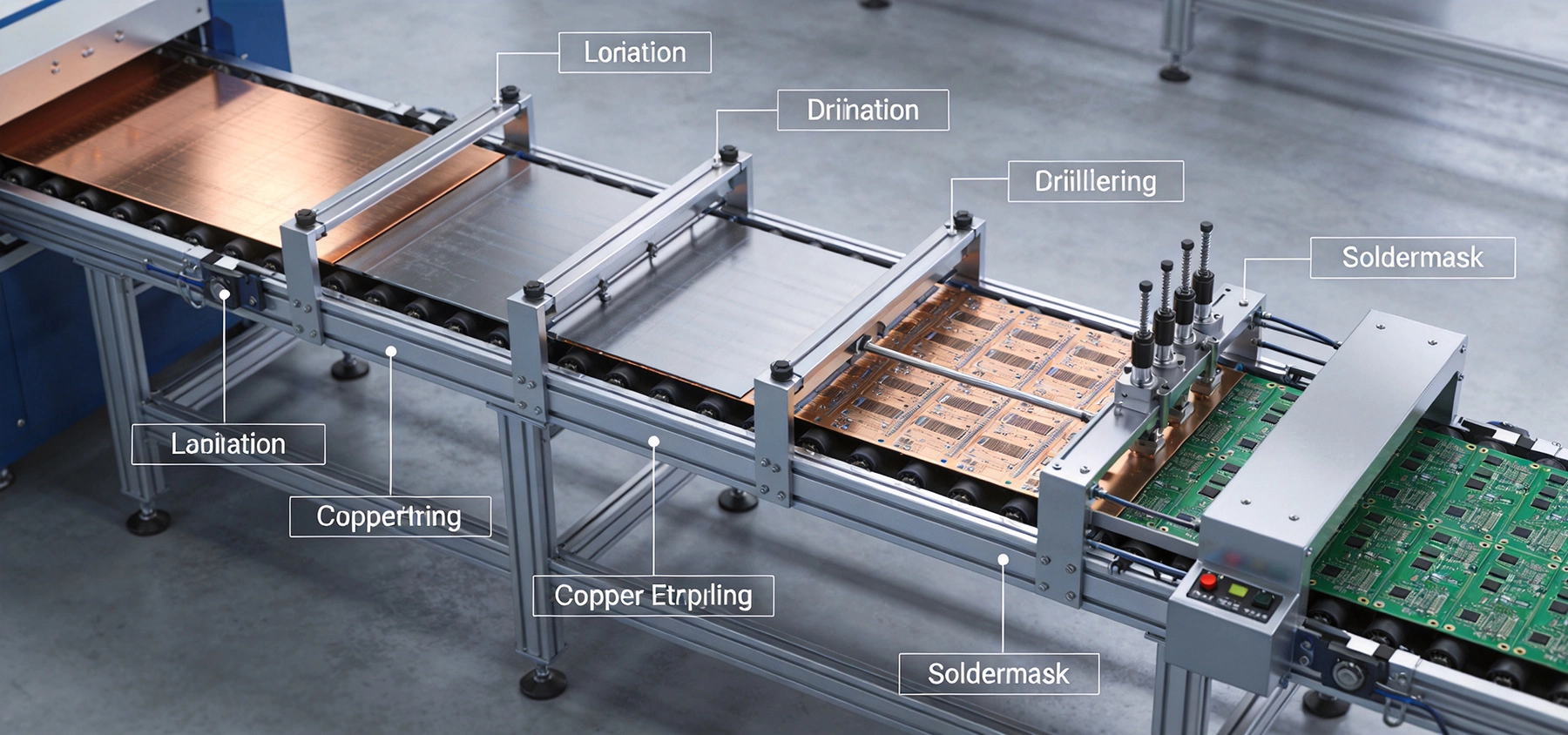
Visualizing the Flow: An Infographic Guide to How Your PCB is MadeSeptember/24/2026You upload your Gerber files, wait a few days, and a finished PCB arrives at your door. But what actually happens in between? Understanding the manufacturing process—really understanding it, step by step—makes you a better designer. When you know how copper is etched, why lamination pressure matte...
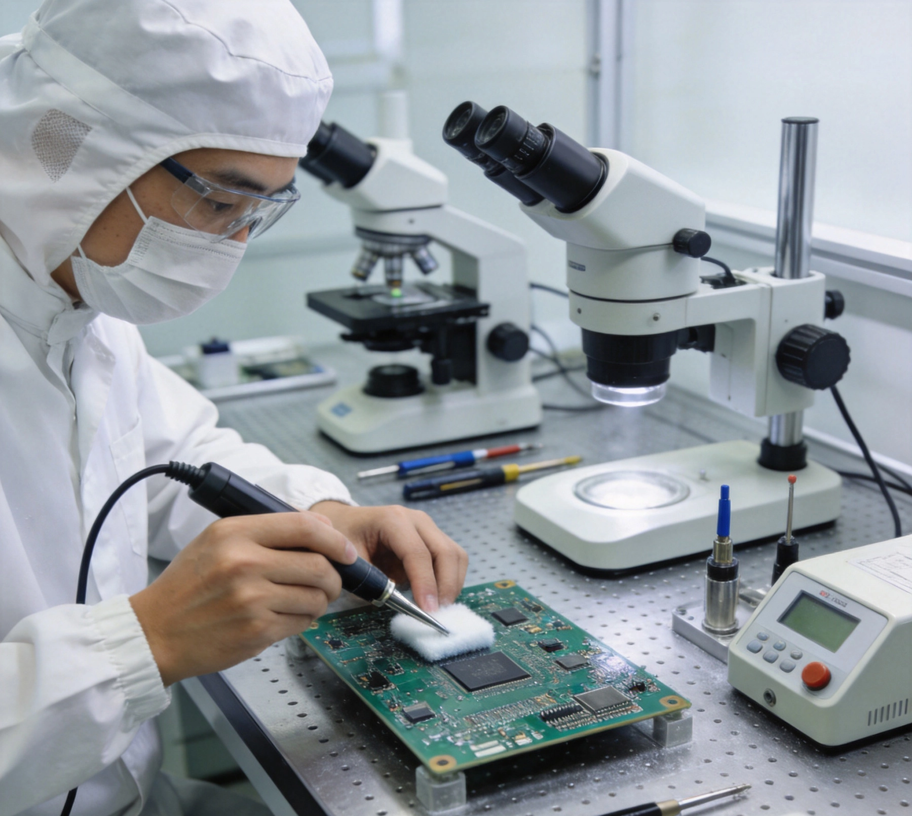
Surface Preparation: The Critical Steps Before Component AssemblySeptember/16/2026Every reliable solder joint begins long before the paste is dispensed or the reflow oven reaches temperature. The quality of the bare printed circuit board surface arriving from fabrication—and the preparation it receives before assembly—determines whether components will form strong, reliable con...
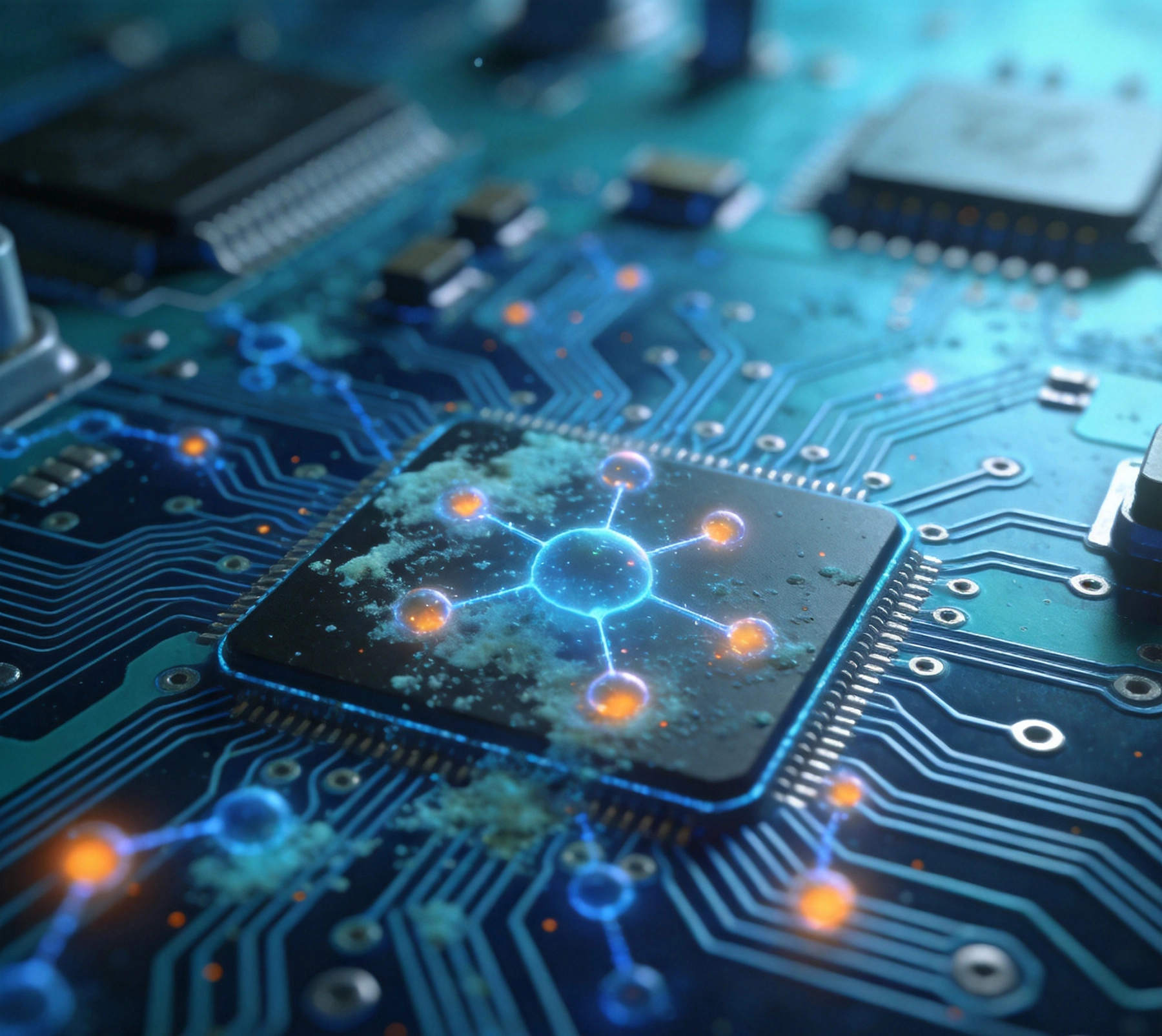
The Chemistry of PCB Cleaning: Why Ionic Contamination MattersSeptember/04/2026When your smartphone drops a call, your car's airbag fails to deploy, or industrial equipment shuts down unexpectedly, you probably don't think "ionic contamination on the PCB." But these invisible residues—the remnants of solder flux, fingerprints, and processing chemicals—cause a surprising numb...
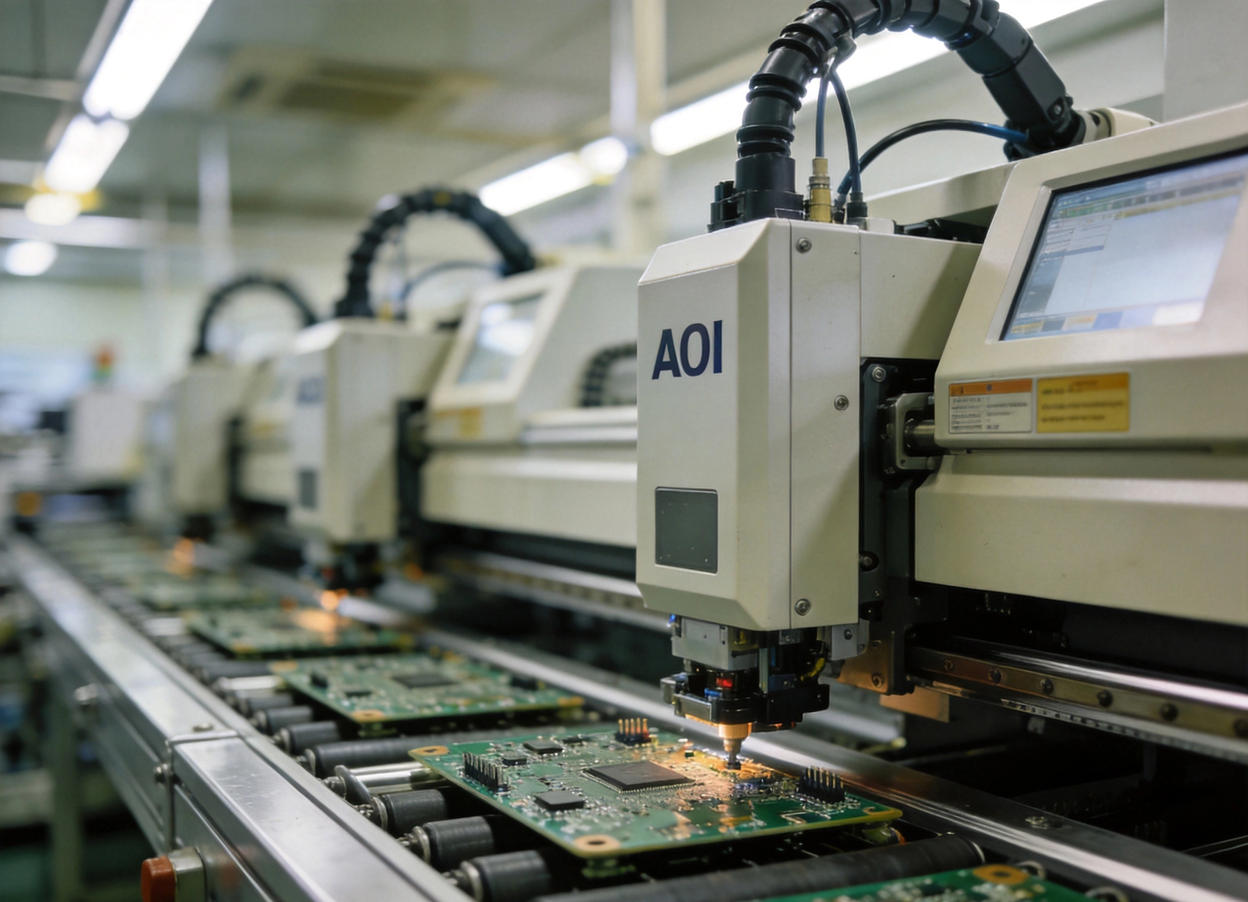
Quality Control 101: AOI, X-Ray, and Electrical Testing in PCB ProductionAugust/10/2026Every PCB that ships to customers should work correctly the first time. Achieving this goal requires systematic quality control at every production stage. Three complementary inspection technologies form the backbone of modern PCB quality assurance: Automated Optical Inspection (AOI), X-ray inspec...
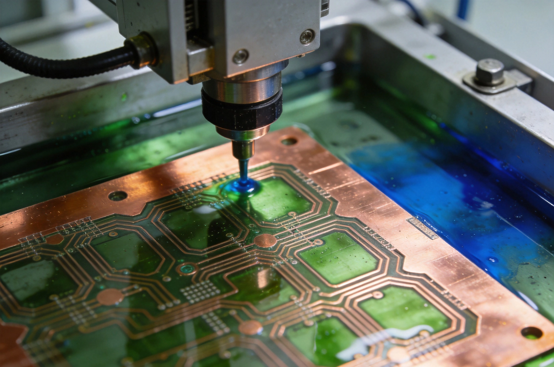
Etching Explained: How Circuit Patterns are Precisely Formed on Copper Clad LaminatesJuly/30/2026Every printed circuit board starts as a blank sheet of copper clad laminate. A thin layer of copper, typically 18 to 70 microns thick, covers an insulating substrate made of fiberglass and epoxy resin. Transforming this blank canvas into the intricate network of conductive traces that carry signal...
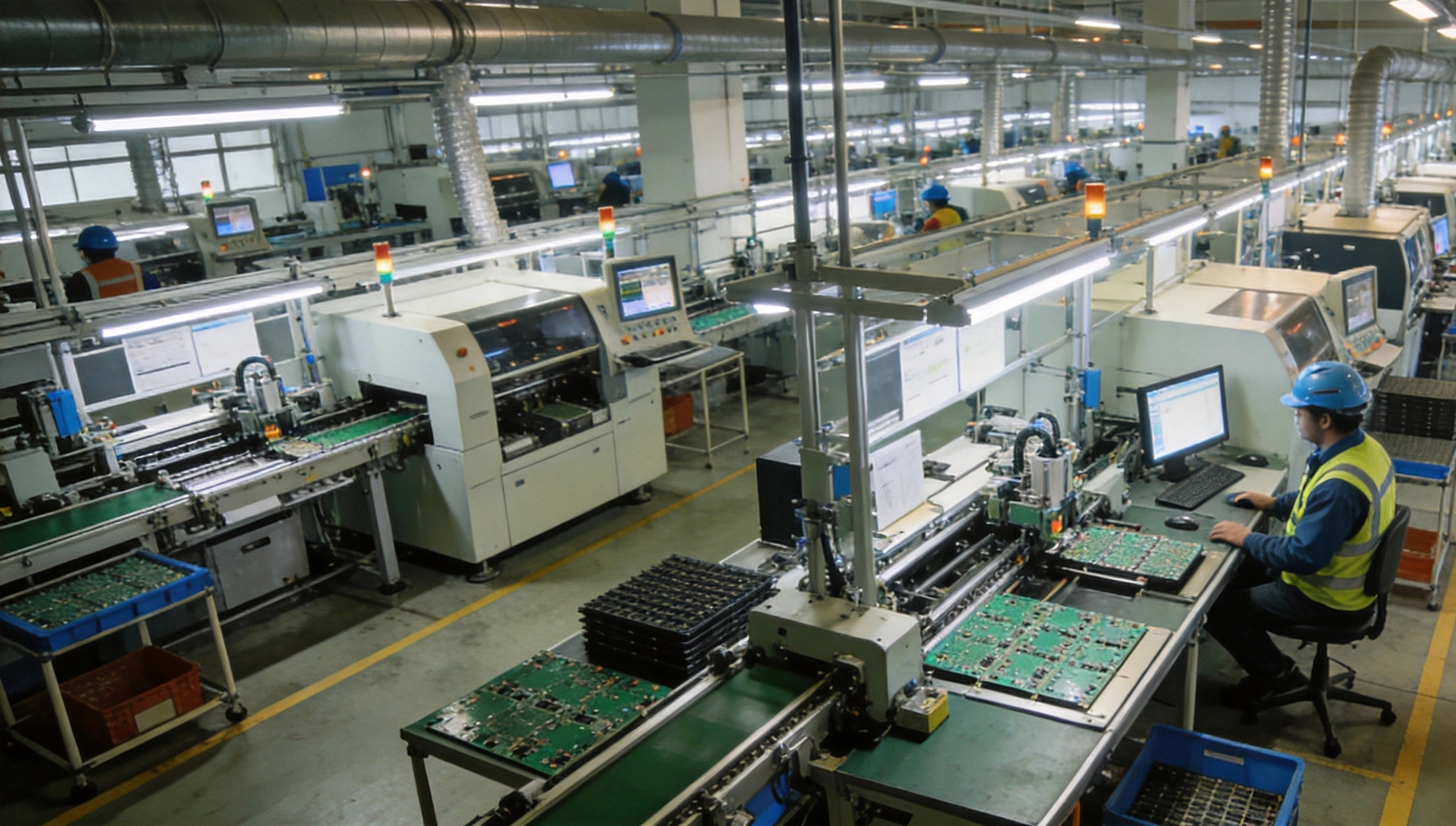
Is PCB Fabrication in China Still the Most Cost-Effective Option? A 2026 AnalysisJuly/27/2026For more than two decades, the economics of PCB fabrication pointed decisively toward China. Lower labor costs, concentrated supply chains, mature manufacturing ecosystems, and favorable trade policies combined to create cost structures that no other region could match. Western electronics compani...
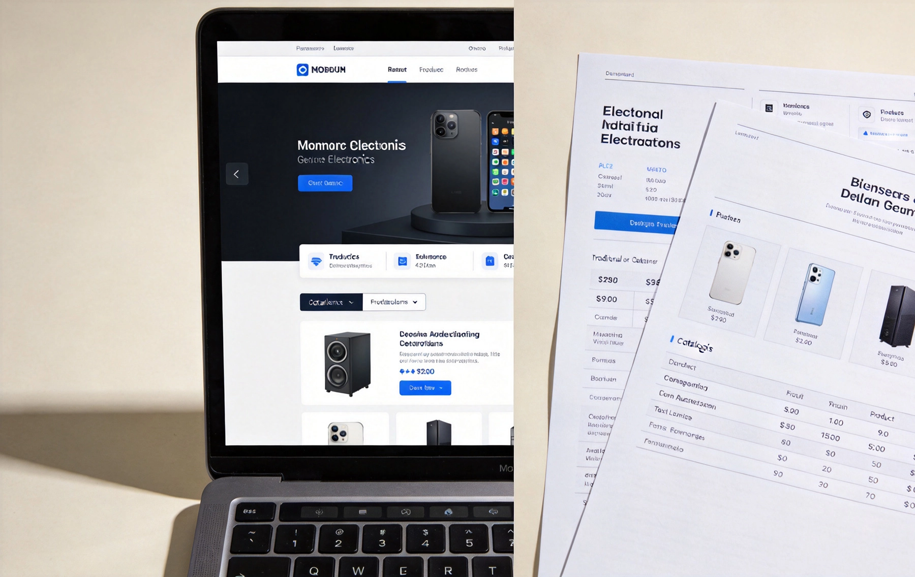
E-Commerce vs. Traditional Sales: How Buying PCB Services Has ChangedJuly/25/2026For most of the electronics industry's history, procuring custom PCBs was a relationship-driven process. Engineers and procurement professionals called sales representatives, waited for quotes that arrived days later, negotiated pricing through back-and-forth emails, and relied on personal connect...
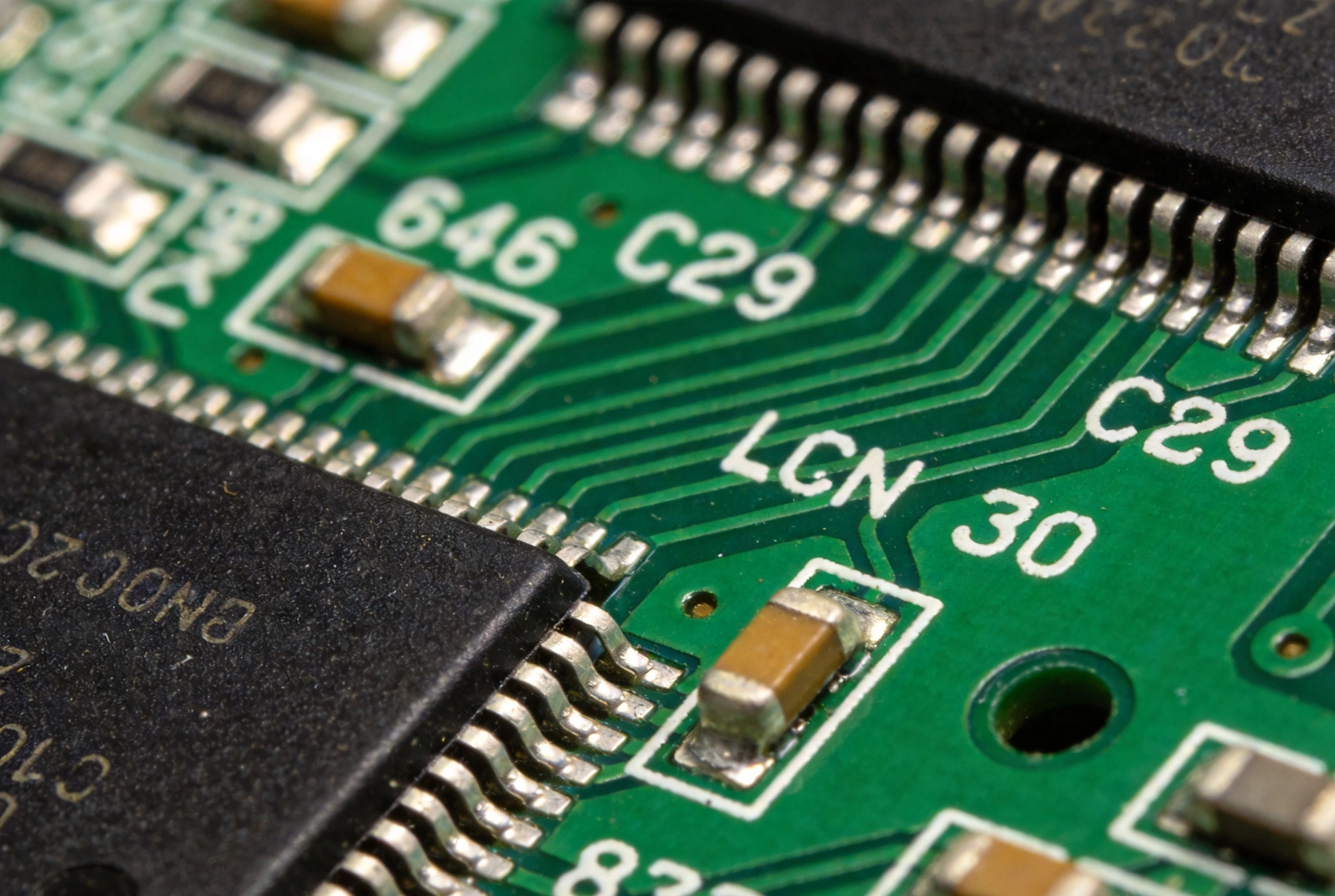
Solder Mask and Silkscreen: More Than Just Aesthetics in the PCB ProcessJuly/20/2026Ask most engineers what solder mask and silkscreen do on a PCB, and you'll get answers focused on appearance. Green boards look professional. White silkscreen makes components readable. These are true observations, but they completely undersell the functional importance of these two process steps....
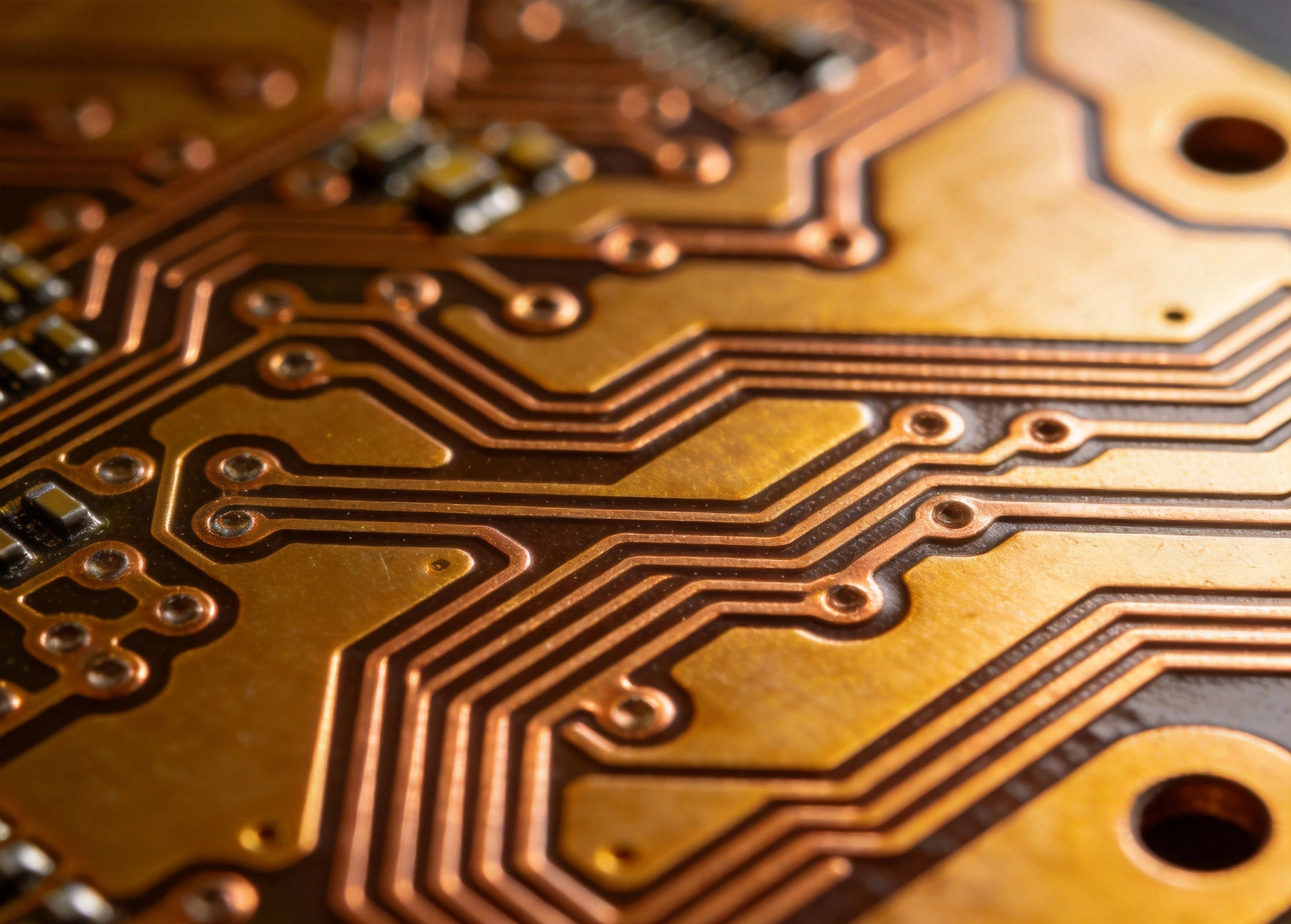
Understanding Copper Plating: Ensuring Connectivity and Durability in PCBsJuly/09/2026Copper is the lifeblood of every printed circuit board. Without copper conductive traces carrying signals and power between components, a PCB would be nothing more than an inert piece of fiberglass. But copper on a raw board is only the starting point. What transforms a bare laminate into a functi...
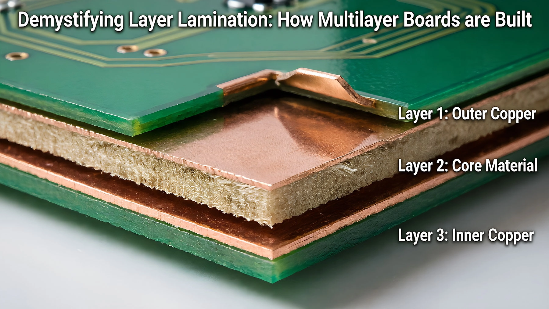
Demystifying Layer Lamination: How Multilayer Boards are BuiltJune/05/2026Have you ever cracked open a modern smartphone or a high-end server and wondered how on earth all those tiny components manage to communicate without a massive tangle of wires? The secret lies hidden right beneath the surface. If you are designing complex electronics, demystifying layer lamination...
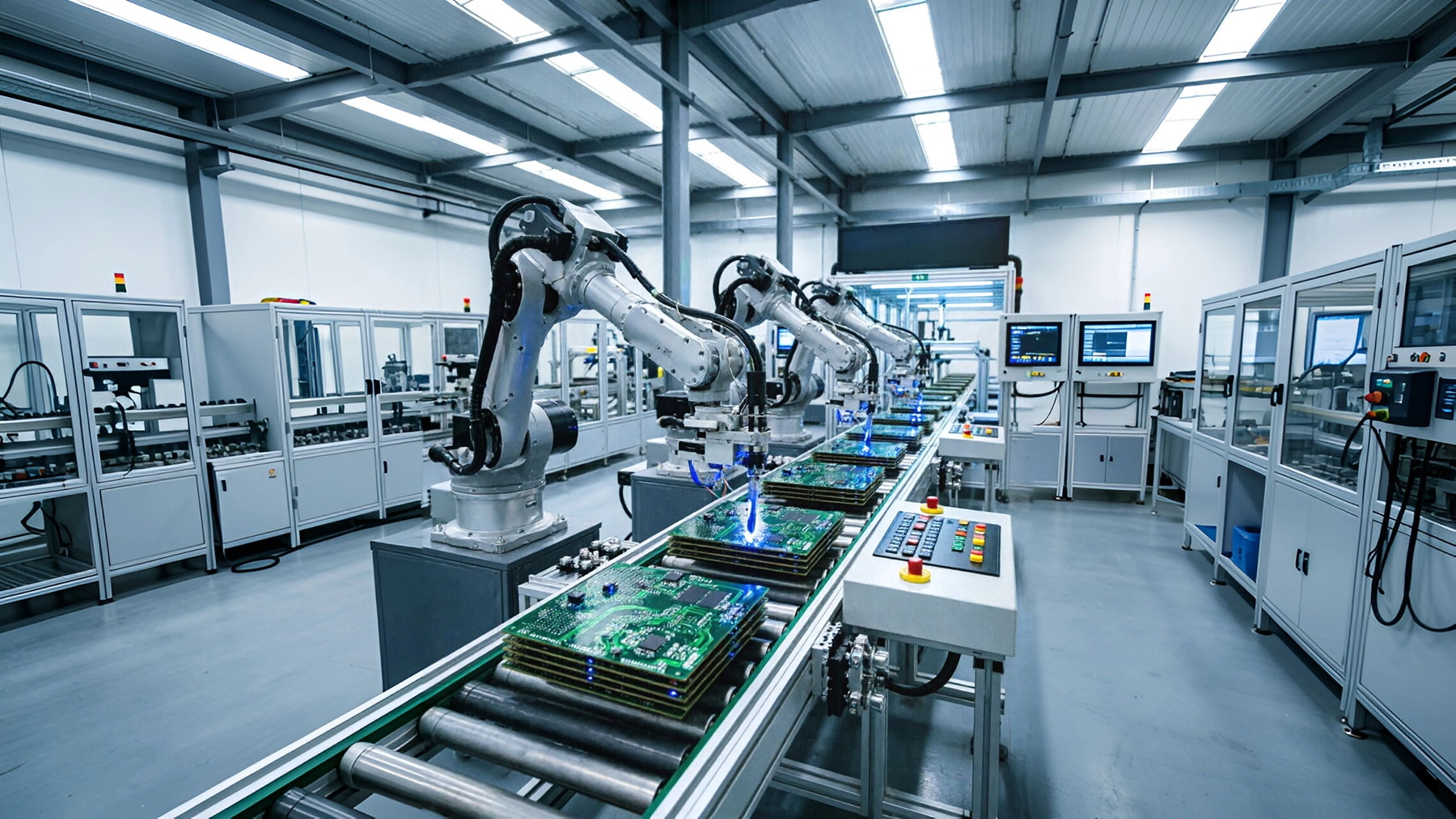
How Automation is Revolutionizing China's PCB SectorJune/03/2026Printed Circuit Boards (PCBs) are universally recognized as the "mother of electronic products." As global demand for AI servers, autonomous vehicles, and 5G devices surges, the traditional manufacturing methods of PCBs are hitting a wall. Enter the smart factory. In recent years, smart factories ...
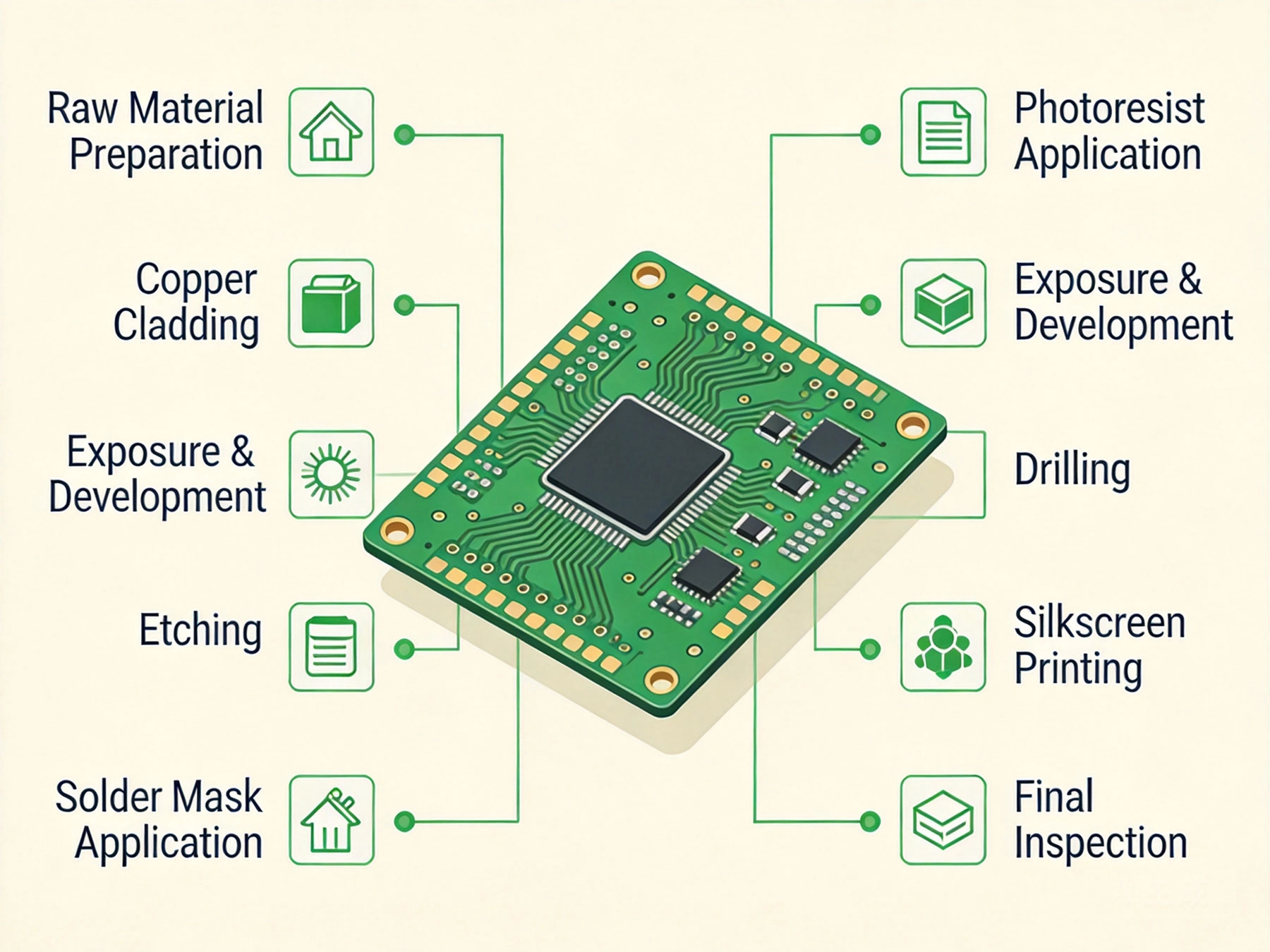
A Step-by-Step Walkthrough of the PCB Fabrication ProcessMay/21/2026Understanding the journey from design files to finished PCBWhat Happens Between Design and DeliveryYou have spent weeks perfecting your PCB design. Your Gerber files are ready, your components are on order, and you are eager to see your creation come to life. But what happens between h...