Open Nav
Have you ever cracked open a modern smartphone or a high-end server and wondered how on earth all those tiny components manage to communicate without a massive tangle of wires? The secret lies hidden right beneath the surface. If you are designing complex electronics, demystifying layer lamination is absolutely essential to your success. It is the foundational process where multiple copper and insulating layers are fused into a single, solid board. In this guide, we will walk through exactly how multilayer boards are built, sharing some real-world factory insights and practical tips to help you avoid costly design mistakes.
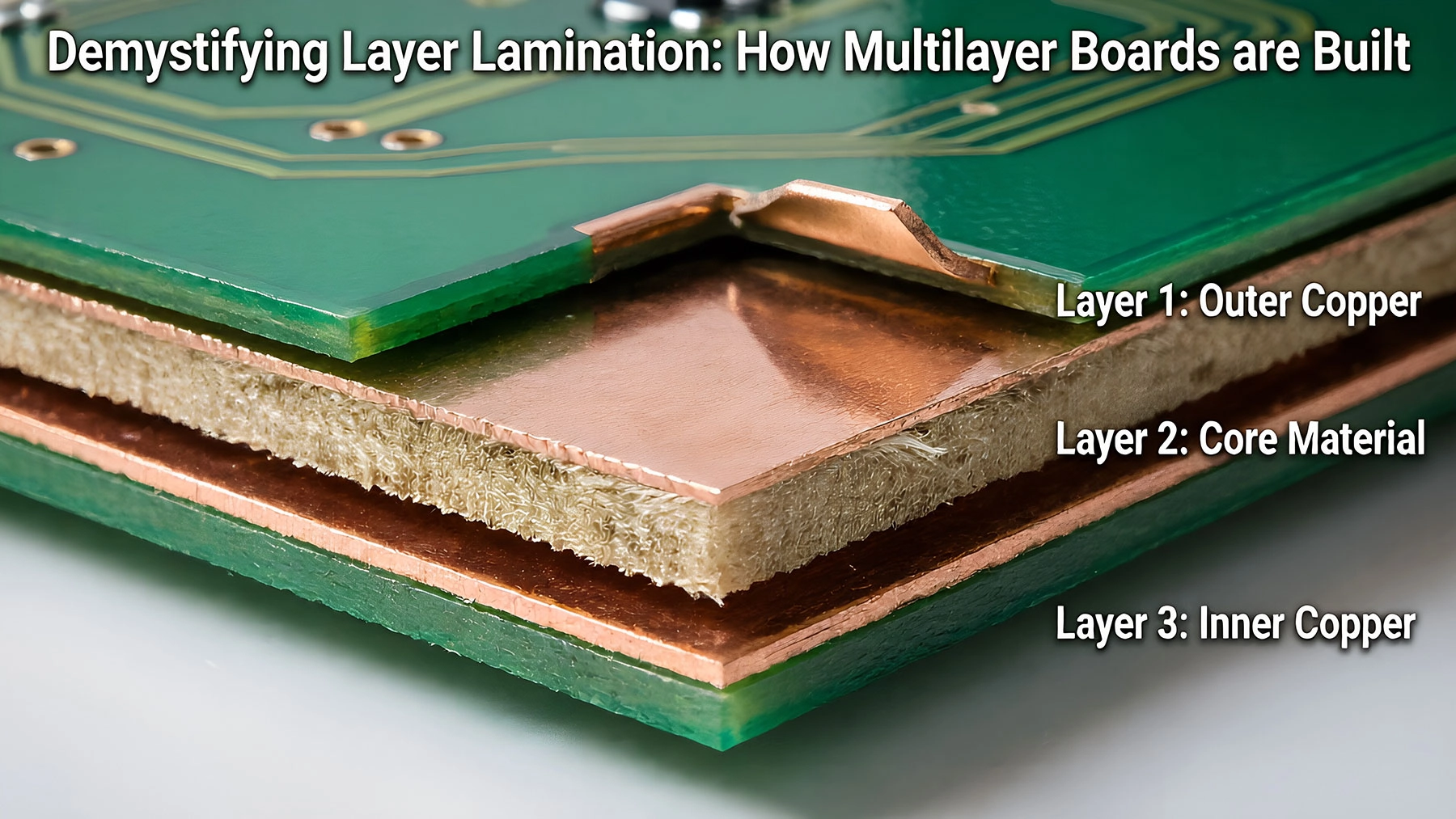
Before we even touch a heating press, we need to understand what we are working with. A lot of beginners think the layers are just glued together like a sandwich, but it is actually a complex chemical reaction. The magic ingredient is called Prepreg (pre-impregnated material). It is basically fiberglass cloth soaked in a resin that is partially cured. When we talk about demystifying layer lamination, understanding Prepreg is step one. It acts as both the insulator and the adhesive. During the heating phase, this resin melts, flows into the empty spaces between the copper traces, and then permanently hardens. Getting the right thickness and resin content here is critical for your board's Impedance Control.
Building a Multilayer Board is a bit like making a very precise, high-tech lasagna. You cannot just throw things in the oven and hope for the best. The stack-up must be perfectly symmetrical to prevent the board from warping during the intense heating and cooling cycles. A typical 4-layer board will have an outer copper foil, a sheet of Prepreg, the inner core (which already has the etched circuits), another sheet of Prepreg, and the bottom copper foil. I have seen so many projects fail because the designer ignored this symmetry rule. If your stack-up is unbalanced, the board will literally bend like a potato chip when it cools down, ruining your alignment and making component assembly a nightmare.
Once the stack is aligned using optical targeting systems, it goes into the lamination press. This is where things get intense. The press applies massive pressure (often hundreds of PSI) and heats the stack to around 170-200°C. But here is a detail many people miss: high-quality manufacturers use a vacuum during this process. Why? Because if air gets trapped between the layers, it creates voids or bubbles. These voids are terrible for electrical performance and can cause delamination later when the board gets hot during soldering. The vacuum pulls out the air while the resin is flowing, ensuring a completely solid, void-free bond. Demystifying layer lamination means knowing that this vacuum step is what separates cheap, unreliable boards from high-reliability aerospace or medical grade PCBs.
After the board comes out of the press, it is a solid block, but the layers are still electrically isolated from each other. To connect them, we have to drill holes and plate them with copper. This is called Plated Through Hole (PTH) technology. The drilling process generates a lot of heat, which can smear the newly cured resin inside the hole. If that smear isn't chemically removed (a process called desmearing), the copper plating won't stick to the inner layers, and you will have an open circuit. It is a delicate balance of mechanical force and chemical cleaning. Always make sure your manufacturer has a robust desmear process, especially if you are using high-Tg materials.
So, how can you make your life easier when designing for this process? First, always consult your fabricator's capability sheet before finalizing your stack-up. They know exactly which Prepreg types they have in stock and what their minimum dielectric thickness can be. Second, keep your copper distribution as even as possible across all layers. Large empty areas can cause the resin to flow unevenly, leading to thickness variations. Third, if you are doing high-speed design, remember that the lamination process slightly squishes the Prepreg. Your calculated trace width for 50-ohm impedance might need a tiny adjustment based on the actual pressed thickness. Communication with your board house early in the design phase will save you weeks of respins.
Demystifying layer lamination is not just about understanding factory equipment; it is about designing better, more reliable products. By respecting the materials, maintaining a symmetrical stack-up, and understanding the thermal and chemical processes involved, you can avoid the most common pitfalls in multilayer Pcb Manufacturing. The next time you hold a dense, high-layer-count board, you will appreciate the incredible engineering that went into fusing those layers together. If you have more questions about Pcb Manufacturing or need help reviewing your stack-up, feel free to reach out or drop a comment below. Happy designing!

How Automation is Revolutionizing China's PCB SectorJune/03/2026
Solder Mask and Silkscreen: More Than Just Aesthetics in the PCB ProcessJuly/20/2026
Understanding Copper Plating: Ensuring Connectivity and Durability in PCBsJuly/09/2026
A Step-by-Step Walkthrough of the PCB Fabrication ProcessMay/21/2026
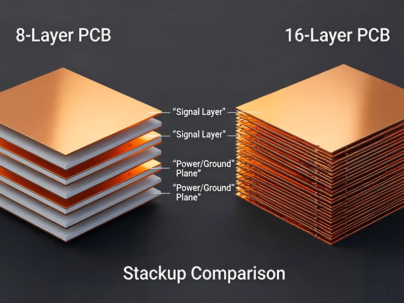
8-Layer vs. 16-Layer: Deciding on the Right Stack-up for Your Multilayer BoardJune/08/2026
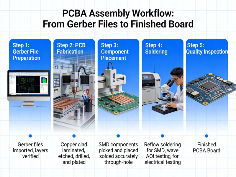
Understanding the PCBA Workflow: From Gerber Files to Finished BoardJune/16/2026
SMT vs THT PCB Assembly in China: Which Technology is Right for Your Project?June/10/2026
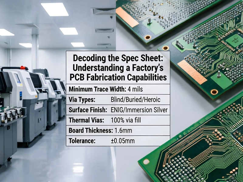
Decoding the Spec Sheet: Understanding a Factory's PCB Fabrication CapabilitiesJune/11/2026