Open Nav
When designing high-speed, high-density electronics, choosing the right Pcb Layer Count is one of the most critical early decisions. The debate between an 8-layer and a 16-layer stack-up is not just about routing space; it is a fundamental trade-off between electrical performance, manufacturing complexity, and budget. While an 8-layer board serves as the workhorse for many advanced applications, stepping up to a 16-layer board enters the realm of elite engineering, typically reserved for systems where performance is non-negotiable.
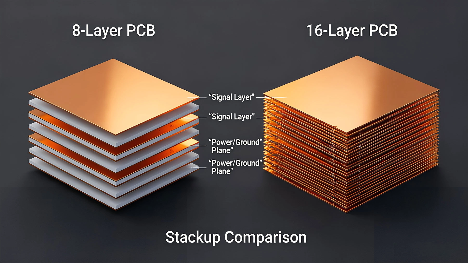
An 8-layer Pcb is often considered the optimal balance for complex digital systems. A standard, highly recommended stack-up for this configuration is TOP-GND-SIG-PWR-GND-SIG-GND-BOTTOM. This structure provides four signal layers sandwiched between multiple ground and power planes. The primary advantage here is excellent Signal Integrity and EMC (Electromagnetic Compatibility) performance. By routing high-speed signals on the inner layers (e.g., L3 and L6), they are fully shielded by adjacent ground planes, creating a stripline structure that minimizes radiation and crosstalk. Furthermore, keeping the power and ground planes tightly coupled (using thin Prepreg layers) provides excellent intrinsic decoupling capacitance. For applications like mid-tier network switches, advanced medical imaging, and industrial controllers, an 8-layer board offers premium performance without the extreme cost penalty of higher layer counts.
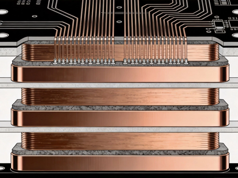
When you step up to a 16-layer board, you are no longer just designing a circuit; you are engineering a complex system. Boards of this magnitude are the backbone of 5G macro baseband processing, high-end core routers, and supercomputer interconnects. A typical 16-layer stack-up might alternate signal, ground, and power layers (e.g., 8 signal layers and 8 plane layers) to provide dedicated, unbroken reference planes for every single high-speed trace. This level of redundancy is required to maintain strict Impedance Control (often 50Ω single-ended or 100Ω differential with ±10% tolerance) across massive routing densities. However, this performance comes at a steep price. A 16-layer board can cost anywhere from 5 to 8 times more than a standard 4-layer board, and the manufacturing yield is significantly lower due to the complexity of aligning and pressing so many layers.
The physical manufacturing of a 16-layer board introduces challenges that simply do not exist at the 8-layer level. The lamination process requires multiple high-pressure, high-temperature cycles. Any microscopic bubble, resin starvation, or layer-to-layer misalignment (registration shift) can result in a total board scrap. Consequently, design rules must be relaxed: you will need larger vias, wider trace-to-pad clearances, and less aggressive aspect ratios. Additionally, the design cycle for a 16-layer board requires senior hardware engineers and extensive Signal Integrity (SI) and power integrity (PI) simulations. An 8-layer board, while still requiring careful planning, is much more forgiving and can be designed and manufactured with significantly faster turnaround times.
Ultimately, the choice between 8 and 16 layers should be driven by your system's electrical requirements, not just routing convenience. If your design features PCIe Gen4/5, DDR4/5 memory, or high-speed SerDes, and you are experiencing severe crosstalk or impedance discontinuities on an 8-layer board, it may be time to upgrade. However, if your 8-layer board is functioning well but you are simply running out of routing channels, consider optimizing your layout, utilizing blind/buried vias, or moving to HDI (High-density Interconnect) technology before committing to the massive cost and schedule overhead of a 16-layer stack-up. Always consult with your Pcb Manufacturer early in the design phase to ensure your chosen stack-up aligns with their fabrication capabilities.
How to Specify Tolerances and Stack-ups for High-Precision Custom PCBsJuly/28/2026
Essential Tips for Your First Custom PCB OrderJune/02/2026
Understanding Copper Plating: Ensuring Connectivity and Durability in PCBsJuly/09/2026
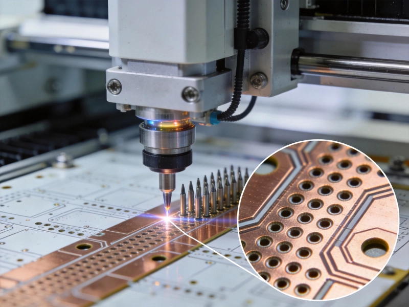
The Art of Drilling: Mechanical vs. Laser Drilling in Modern PCB ManufacturingJune/26/2026
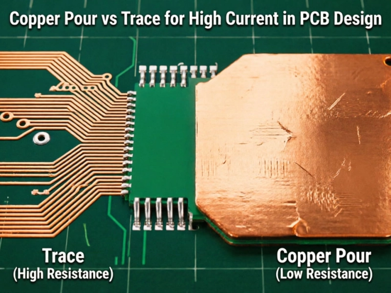
Copper Pour vs Trace for High Current: Optimizing PCB Power Delivery and Thermal ManagementJune/11/2026

E-Commerce vs. Traditional Sales: How Buying PCB Services Has ChangedJuly/25/2026
Heavy Copper PCBs: Capabilities for High-Current and Power ElectronicsJuly/14/2026

Inventory Management and Kitting: Streamlining Your Supply Chain with PCB ServicesJuly/15/2026