Open Nav

As digital systems push into ever-higher frequencies, the principles that once applied only to RF design now govern everyday PCB layouts. Signal Integrity—once a concern primarily for telecommunications and radar systems—has become central to everything from smartphone processors to automotive electronics. When edge rates shrink below a nanosecond and clock frequencies climb past several gigahertz, a PCB trace is no longer just a conductor; it's a transmission line.
Managing Signal Integrity in high-speed multilayer PCBs requires a systematic approach that addresses Impedance Control, stackup design, routing strategies, and electromagnetic compatibility. Understanding these principles enables engineers to design boards that perform reliably in demanding applications without requiring multiple design iterations.
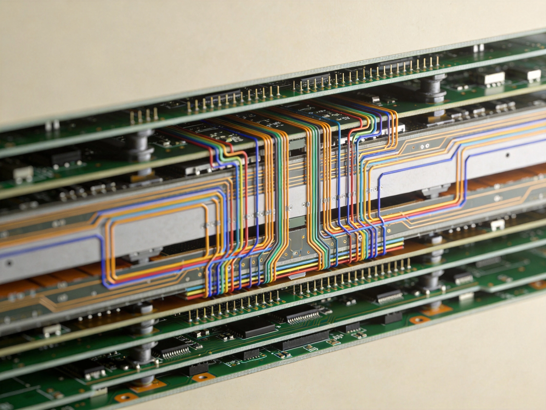
Signal integrity encompasses all aspects of signal quality as it propagates through a system. In ideal circuits, a signal at the driver appears unchanged at the receiver. In real high-speed circuits, signals degrade through multiple mechanisms:
When a signal encounters an impedance change—such as a trace width transition, a via, or a connector—some energy reflects back toward the source. These reflections distort the original signal waveform. If reflections arrive at the receiver during signal transitions, they can cause false triggering, timing errors, or data corruption.
At low speeds, reflections are negligible because signal transitions are slow compared to propagation delays. At high speeds, reflection energy arrives during the critical switching window, causing intersymbol interference and reducing timing margin.
Adjacent traces couple through both capacitive and inductive mechanisms. When one trace switches, it induces noise on neighboring traces. At high speeds, this crosstalk can exceed receiver noise margins, causing errors in seemingly unrelated signals.
Crosstalk increases with faster edge rates, longer parallel runs, and closer trace spacing. Managing crosstalk requires careful attention to routing geometry and layer assignments.
Conductor resistance, dielectric absorption, and skin effect losses attenuate signals as they propagate. At high frequencies, these losses become significant, reducing signal amplitude and slowing edge rates. Excessive attenuation can prevent signals from reaching receiver thresholds.
Signal integrity problems affect timing in multiple ways. Reflections can cause setup and hold violations. Crosstalk-induced jitter reduces timing margin. Attenuation slows edge rates, increasing propagation delay. These effects accumulate, potentially causing system-level timing failures.
Controlled Impedance is the foundation of high-speed signal integrity. A Controlled Impedance trace maintains consistent characteristic impedance along its length, minimizing reflections and enabling predictable signal propagation.
Characteristic impedance (Z0) is determined by trace geometry and material properties. For a microstrip configuration (trace on outer layer with ground plane beneath):
Z0 depends on trace width, copper thickness, distance to the reference plane, and Dielectric Constant of the substrate. For stripline configurations (trace between two reference planes), impedance depends on similar factors but with different relationships.
Standard impedance values are 50Ω for single-ended signals and 100Ω for differential pairs, though other values are common in specific applications. The key is maintaining impedance consistency rather than achieving any particular value.
Manufacturing tolerances affect impedance accuracy. Typical impedance tolerance is ±10% for standard processes, with ±5% achievable through controlled processes. This tolerance includes variations in:
Design for achievable tolerances rather than assuming perfect impedance. Account for worst-case impedance variations when analyzing signal integrity.
Layer stackup is perhaps the most critical decision in high-speed multilayer Pcb Design. A well-designed stackup enables good signal integrity; a poor stackup makes signal integrity difficult or impossible to achieve.
Every high-speed signal layer needs an adjacent reference plane. This plane provides:
Best practices for reference planes:
Symmetric or balanced stackups help prevent warpage during manufacturing. A balanced stackup has identical layer arrangements above and below the centerline. For signal integrity, symmetry also means:
4-Layer Stackup: Signal-Ground-Power-Signal. Simple but effective for moderate-speed designs. Signal layers reference the adjacent plane. Limited routing density but straightforward impedance control.
6-Layer Stackup: Signal-Ground-Signal-Signal-Power-Signal. Provides more routing layers with controlled impedance. Inner signal layers are stripline configuration; outer layers are microstrip.
8-Layer Stackup: Signal-Ground-Signal-Power-Ground-Signal-Ground-Signal. Multiple ground planes provide excellent shielding between signal layers. Suitable for high-density, high-speed designs.
10+ Layer Stackup: Alternating signal and ground/power layers with additional dedicated ground planes. Used for very high-speed, high-density designs requiring maximum routing channels with minimal crosstalk.
Material choice affects both impedance and signal loss:
Material selection involves tradeoffs between performance, cost, and manufacturability. High-performance materials cost more and may require specialized processing.
Single-ended signals use one conductor referenced to ground. Most digital interfaces (SPI, UART, control signals) use single-ended signaling, though high-speed versions increasingly require controlled impedance.
Maintain consistent trace width along controlled impedance paths. Changes in width create impedance discontinuities. When width changes are unavoidable, use gradual tapers rather than abrupt transitions.
Return current flows in the reference plane beneath the trace. Any disruption to this return path creates inductance and impedance discontinuity. Common issues include:
For timing-critical signals, length matching ensures signals arrive simultaneously. However, electrical length depends on propagation velocity, which varies with dielectric constant. Microstrip and stripline traces have different propagation velocities; account for this when matching lengths across layer types.
Differential signaling uses two complementary signals that carry equal and opposite voltages. Differential pairs offer superior noise immunity and are essential for high-speed interfaces like USB, PCIe, HDMI, and DDR.
Differential impedance depends on both trace geometry and spacing between pair members. Tighter coupling (closer spacing) lowers differential impedance. The relationship between single-ended and differential impedance is:
Zdiff ≈ 2 × Zse × (1 - k)
Where k is the coupling coefficient. Tight coupling increases k, reducing differential impedance for the same single-ended impedance.
Maintain consistent spacing between pair members. Spacing changes affect differential impedance and can cause reflections. Choose a spacing appropriate for your impedance target and maintain it consistently.
Common practice uses edge-to-edge spacing equal to or less than trace width. Tighter coupling provides better noise rejection but makes routing more challenging.
Length mismatch within a differential pair causes mode conversion—some signal energy converts from differential to common mode. This conversion reduces signal integrity and increases EMI. Typical length matching tolerance is ±5 mil for moderate-speed signals, tightening to ±2 mil for very high-speed designs.
Length matching often requires adding serpentine routing (meanders) to the shorter trace. Place meanders near the mismatch source rather than arbitrarily in the routing.
When differential pairs transition between layers, both traces should transition together with their ground via (if used) centered between them. Maintain pair spacing through the via region. Some designs use differential vias specifically designed for pair transitions.
Vias create unavoidable impedance discontinuities. Understanding via effects helps minimize their impact on signal integrity.
When a via passes through multiple layers, the unused portion creates a stub. This stub acts as a transmission line stub antenna, causing reflections at frequencies where stub length approaches quarter-wavelength. For high-speed signals:
Vias have higher inductance than traces due to their geometry. This inductance causes impedance discontinuity at the via. Minimize via impact through:
When signals transition layers, return current must transition too. Without a nearby ground via, return current must find an alternate path, creating a large current loop and inductance. Place ground vias within 50 mil of signal vias for moderate-speed signals, closer for very high-speed designs.
Crosstalk occurs through capacitive and inductive coupling between adjacent traces. Effective management reduces coupling below problematic levels.
Wider spacing reduces crosstalk. The 3W rule (spacing equal to 3× trace width) significantly reduces crosstalk for typical geometries. For critical signals, 5W spacing provides even better isolation.
Adjacent signals on different layers can couple significantly. Avoid routing signals directly parallel on adjacent layers. If parallel routing is unavoidable, ensure signals are orthogonal (horizontal on one layer, vertical on the next).
Ground traces between sensitive signals provide shielding. However, guard traces must connect to ground at regular intervals to be effective. A guard trace floating or connected only at one end provides minimal benefit.
Assign critical signals to inner stripline layers sandwiched between ground planes. This configuration provides natural shielding from both directions. Use outer microstrip layers for less critical signals or where connector escape routing requires it.
Power distribution network (PDN) design directly impacts signal integrity. Inadequate PDN causes power supply noise that couples into signals, while poor signal integrity causes current transients that stress the PDN.
High-speed ICs draw current transients during switching. Decoupling capacitors provide local charge storage to supply these transients. Effective decoupling requires:
Adjacent power and ground planes form a parallel plate capacitor. This capacitance provides very low-inductance decoupling at high frequencies. Plane capacitance is most effective when planes are closely spaced (2-4 mil dielectric).
Signal return current flows in the nearest reference plane. If that plane is a power plane rather than ground, return current must find a path to ground through decoupling capacitors. This requirement motivates dedicated ground planes adjacent to signal layers.
Signal integrity simulation identifies problems before manufacturing. Tools range from simple impedance calculators to full 3D electromagnetic simulators. Typical simulation workflow:
Simulation accuracy depends on model quality. Use manufacturer IBIS models for drivers and receivers. Verify PCB material properties with your fabricator.
Post-layout verification includes:
Measurement requires test structures designed into the board. Include impedance test coupons, via test structures, and accessible measurement points in production designs.
Engineers often focus on signal routing while neglecting return paths. Remember that every signal has an equal and opposite return current. Disrupted return paths cause EMI and signal integrity problems.
Solution: Plan return paths as carefully as signal paths. Ensure ground vias accompany layer transitions. Avoid routing signals across split planes.
Impedance variations from inconsistent trace width, spacing, or dielectric thickness cause reflections that degrade signal quality.
Solution: Use consistent trace geometries. Verify impedance-critical traces for width and spacing changes. Work with your fabricator to understand achievable tolerances.
Skipping simulation or using inadequate tools leads to problems discovered only in Prototype testing.
Solution: Simulate critical signals before committing to layout. Use appropriate simulation depth for each design—simple impedance calculation for moderate-speed signals, full electromagnetic simulation for cutting-edge designs.
Signal integrity and impedance control are no longer optional considerations—they're essential requirements for modern digital design. As frequencies continue to rise, these requirements will become even more stringent.
Successful high-speed Pcb Design requires attention to fundamentals: proper stackup design, controlled impedance routing, careful via placement, and adequate crosstalk management. These elements work together to create boards that perform reliably in demanding applications.
The investment in understanding signal integrity principles pays dividends across all high-speed designs. Each project builds expertise that makes subsequent designs more efficient. Working closely with your PCB fabricator—communicating impedance requirements clearly and understanding their process capabilities—ensures that designed-for performance translates into manufactured reality.
Remember that signal integrity is a system-level concern. Board design, component selection, and system integration all contribute to signal quality. Addressing these elements systematically yields designs that perform reliably without expensive redesign cycles.
Custom Surface Finishes: Choosing Between ENIG, HASL, OSP, and Immersion SilverSeptember/14/2026

Emergency PCB Runs: Strategies for Getting Boards Fast Without Sacrificing ReliabilityJuly/08/2026

Understanding the Basics of PCB Production China: From Gerber Files to Finished BoardsOctober/16/2026

Best Practices for Preparing Files for Expedited PCB ManufacturingJuly/29/2026
Why Quick Turn PCB Fabrication is Critical for R&D TeamsMay/21/2026

Questions to Ask Before Placing a Rush Order for PCB FabricationSeptember/15/2026
How to Specify Tolerances and Stack-ups for High-Precision Custom PCBsJuly/28/2026

Comparing Traditional vs. Digital Quick Turn PCB ServicesJuly/18/2026