
Fit more into less. That's the central promise behind HDI PCB Fabrication, and it's reshaping what's possible in compact Electronics Design. From the smartwatch on your wrist to the vehicle control modules under the hood, High Density Interconnect technology is quietly powering the devices we rely on every day.
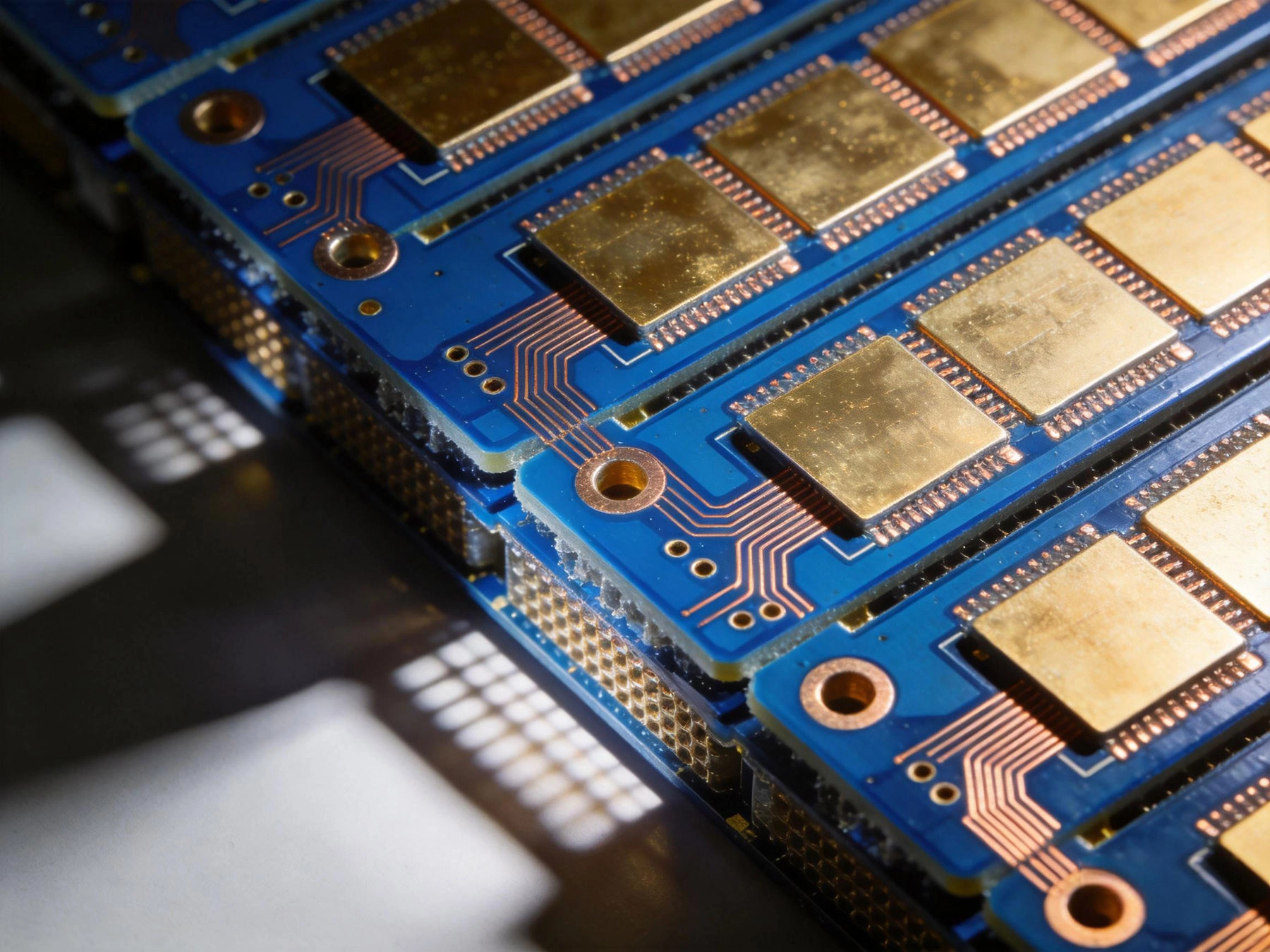
Picture two circuit boards handling the same tasks. One fills a smartphone. The other barely fits inside a Bluetooth earbud. The difference? One was built with traditional Multilayer Pcb technology. The other used HDI PCB Fabrication to achieve the same—or better—performance in a fraction of the space.
HDI—short for High Density Interconnect—isn't some experimental concept sitting in a research lab. It's in your phone. It's in medical sensors. It's running inside automotive controls and industrial IoT devices. If you're designing anything that needs to be smaller, lighter, and more capable, understanding HDI's advantages isn't optional—it's essential.
Traditional PCBs rely on through-hole vias to connect layers. These are relatively large holes drilled through the entire board—simple to manufacture, but they eat up board space and create electrical stubs that degrade high-frequency signals.
HDI takes a different path. It uses micro-vias—laser-drilled holes typically between 0.10mm and 0.25mm in diameter—that connect only adjacent layers. A micro-via that's 0.15mm wide takes up roughly 28 times less board area than an 0.8mm traditional via. On a complex design with hundreds of connections, the space savings compound quickly.
But HDI isn't just about smaller holes. It fundamentally changes the routing philosophy. Instead of forcing all major routing to outer layers, HDI distributes connections throughout all layers. Components on both sides of the board can interconnect freely, and signals take shorter, cleaner paths between layers.
Here's what a production-ready HDI board typically delivers:
Squeeze more out of every square millimeter. That's the number-one reason designers adopt HDI, and it's a compelling one.
By replacing large through-hole vias with micro-vias, eliminating unnecessary annular rings, and distributing routing across more layers, HDI enables 30% to 40% board size reduction compared to equivalent traditional multilayer designs. The functionality stays the same—or increases—while the board shrinks.
This is why Apple moved to HDI in iPhones years ago, why the latest TWS earbuds can pack noise cancellation and wireless charging into a casing smaller than a wine cork, and why medical implant controllers keep shrinking while adding features.
Here's something counterintuitive: making the board smaller sometimes makes it perform better. That's exactly what happens with signal quality in HDI.
Traditional through-hole vias create stubs—unused sections of barrel that resonate at high frequencies, reflecting signals and adding noise. HDI's blind and buried micro-vias don't have this problem. The signal path between layers is short and direct, minimizing inductance and parasitic capacitance.
The result? Measurably better Signal Integrity for DDR5 memory interfaces, PCIe 5.0 buses, 5G RF paths, and any application pushing past 1 GHz. Engineers frequently report 50% or greater improvements in signal margin after migrating to HDI.
Smaller boards naturally weigh less. But HDI goes further. The thinner dielectric materials used in HDI construction allow for lighter substrates without sacrificing mechanical robustness. Some HDI designs replace standard FR-4 with advanced composites that are both lighter and more thermally stable.
In aerospace and drone applications, every gram counts toward either additional payload capacity or extended battery life. A 35% reduction in PCB weight translates directly into longer flight times or more sensors. In medical wearables, it means devices patients actually tolerate wearing.
Thermal headaches often come with miniaturization. Pack components closer together and heat concentrates. But HDI actually helps here through two mechanisms.
First, micro-vias create shorter thermal conduction paths from hot components to internal thermal planes—heat escapes faster. Second, component density places heat sources in more集中 zones, which sounds bad but actually simplifies thermal design. Instead of chasing scattered hot spots across a large board, engineers can target one well-defined area with a dedicated heat spreader or thermal interface material.
When you remove the constraint of routing everything through outer layers, surprising things happen. Components that previously had to be placed far apart due to trace routing constraints can now sit next to each other. Signal paths get shorter. Impedance Control becomes more consistent.
Any-layer HDI construction (ALIVH) takes this further: any layer can connect to any other layer through buried micro-vias. This means a 12-layer HDI board can achieve routing density equivalent to a 20-layer traditional board, at lower cost and with better electrical performance.
Not all HDI boards are equal. The construction approach—called the stack-up—determines how many layers of micro-vias exist and how they connect. Choosing the right one is one of the most consequential decisions in an HDI design.
| HDI Stack-Up | How It Works | Best For |
|---|---|---|
| 1st Order (1-N-1) | One micro-via layer, connecting each outer layer to one adjacent internal layer | Smartphones, tablets, cost-sensitive designs |
| 2nd Order (2-N-2) | Two micro-via layers, enabling connections spanning two internal layers | Advanced smartphones, automotive ECUs, complex modules |
| 3rd Order & Beyond | Three or more micro-via layers, maximum layer skipping capability | AI processors, network ASICs, high-density modules |
| Any-Layer (ALIVH) | Every internal layer can connect to every other layer via Buried Vias | Ultra-miniature devices, hearables, medical implants |
Most commercial products land in the 1st or 2nd order category. Any-layer HDI delivers the highest density but costs more and requires more advanced manufacturing. Don't pay for any-layer unless your design genuinely needs it—1st order HDI often captures 80% of the density benefit at significantly lower cost.
HDI is powerful. It's also more expensive than traditional Pcb Fabrication, typically adding 20% to 50% to board cost. Before committing, be honest about whether your project actually needs it.
HDI is the right choice when:
Stick with traditional Multilayer Pcb when:
"After switching our GPS tracker module to 2nd order HDI, we removed an entire PCB layer, shrank the board by 38%, and—unexpectedly—reduced electromagnetic emissions enough to pass FCC testing on the first attempt. The Signal Integrity improvement was a happy accident that saved us weeks." — Hardware Lead, Consumer IoT Company
HDI pushes manufacturing equipment to its limits. Being aware of the challenges upfront prevents painful surprises later in the development cycle.
These manufacturing demands are exactly why HDI costs more. The equipment is specialized, the processes are exacting, and the yield rates—while good at experienced shops—generally run lower than standard multilayer production. Choose your manufacturer carefully and share your design files early for Dfm Review.
If you're new to HDI, here's a condensed checklist from engineers who've been through it:
The trajectory is clear: devices keep shrinking, frequencies keep climbing, and component density keeps increasing. HDI is growing to meet these demands.
Some directions worth tracking:
For designers working on the next generation of compact electronics, HDI isn't just a manufacturing option—it's increasingly the baseline expectation. Understanding its advantages and limitations now puts you ahead of the curve.
HDI Pcb Fabrication transforms what's possible in compact electronics. Whether you're building wearables, automotive modules, medical devices, or IoT hardware, the size, signal, and thermal benefits are within reach. Talk to an experienced HDI manufacturer to see how it applies to your specific requirements.
Production-ready micro-vias can reach 0.10mm today, with some advanced shops hitting 0.075mm in controlled environments. Most standard HDI production targets 0.15mm to 0.20mm for the best balance of capability and yield.
Per board, yes—typically 20% to 50% more. But HDI often reduces the total layer count, simplifies assembly, and shrinks the board enough to lower overall system cost. The real comparison is total product cost, not board cost alone.
Mostly yes. Surface Mount assembly works fine, though paste registration tolerance should be tighter and reflow profiles may need adjustment for thinner HDI substrates. Through-hole components remain compatible, though placement strategies differ due to higher density.
Not strictly necessary, but strongly recommended. 5G mmWave frequencies demand excellent signal integrity and Controlled Impedance—HDI's short, stub-free via paths deliver exactly that. Many 5G modules wouldn't fit the required RF performance in a traditional board without becoming impractically large.
X-ray Inspection is the standard method for HDI. It reveals via barrel fill quality, registration accuracy, and hidden defects that optical inspection misses. Ask your manufacturer about their X-ray inspection protocol and acceptance criteria before placing your order.
Reducing Supply Chain Friction: Why Integrated Fab and Assembly Saves TimeJune/29/2026
Applications Driving the Demand for HDI PCBs: From Smartphones to Medical DevicesSeptember/17/2026
Why Startups Rely on Quick Turn Fabrication to Secure Funding FasterAugust/08/2026

Rigid-Flex and Flexible PCBs: Unlocking New Possibilities with Custom DesignsJuly/17/2026
Common Pitfalls in Custom PCB Fabrication and How to Avoid ThemAugust/07/2026
How to Specify Tolerances and Stack-ups for High-Precision Custom PCBsJuly/28/2026

The Rise of Smart Factories: How Automation is Revolutionizing China's PCB SectorJune/16/2026
Understanding Lead Times: What to Expect When Ordering from Chinese PCB MillsAugust/06/2026