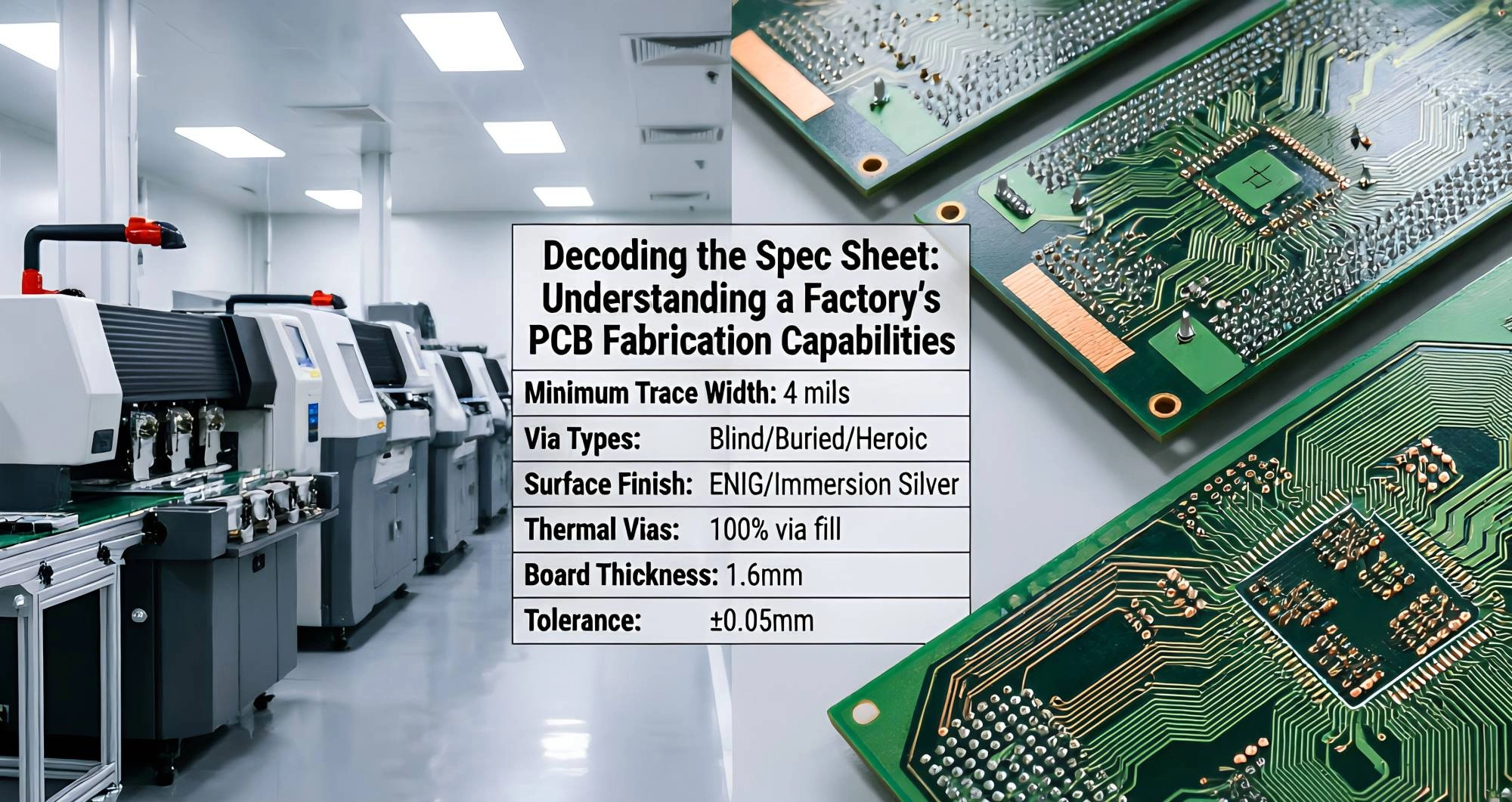
If you are a hardware engineer or a procurement specialist, you have probably stared at a multi-page PDF from a
Pcb Manufacturer and felt completely overwhelmed. A factory's capability spec sheet is essentially their resume. It tells you exactly what they can build, what tolerances they can hold, and where their absolute limits lie. Decoding the Spec Sheet: Understanding a Factory's
Pcb Fabrication Capabilities is not just about reading numbers; it is about matching those numbers to your product’s actual needs without overpaying for features you don't require.
I once worked on a consumer IoT device where we blindly chose a vendor based on their advertised "high-end" capabilities. We ended up paying a premium for 12-layer Any-layer HDI technology when our design actually only required standard 8-layer sequential lamination. By understanding how to read these spec sheets properly, you can avoid costly mistakes and streamline your
Supply Chain.

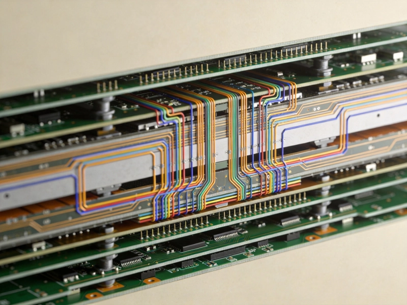
Layer Count and Board Architecture
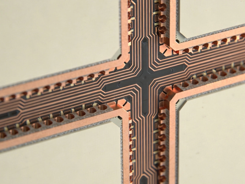
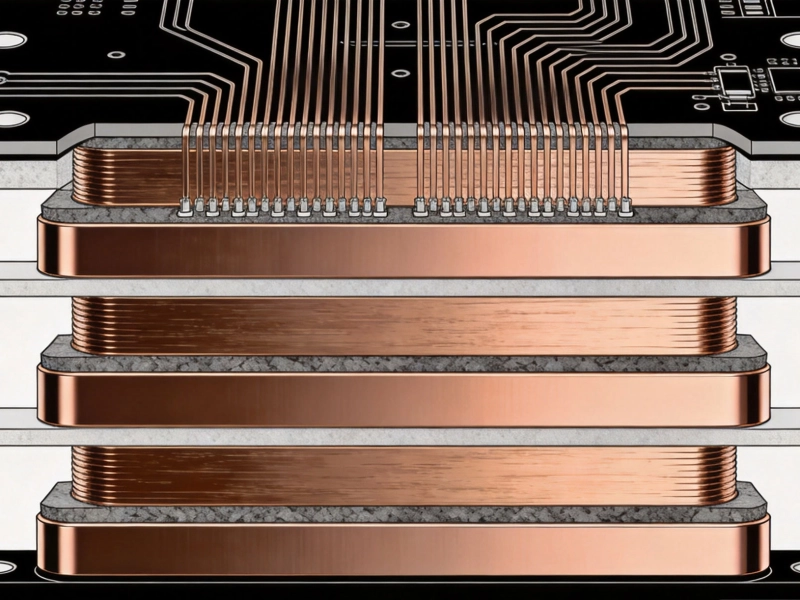
The most obvious metric on any spec sheet is layer count. But don't just look at the maximum number. You need to understand the architecture. Can the factory handle standard
Multilayer Boards, or do they support
High-density Interconnect (HDI)?
Look closely at terms like "Any-layer," "Backdrilling," "Blind/Buried Vias," and "Resin-filled Vias (POFV)." If your spec sheet mentions 20:1 aspect ratios or mechanical microvias, you are dealing with an advanced facility capable of high-speed computing or ADAS domain controllers. For basic consumer electronics, standard through-hole vias and inner layers are perfectly fine and significantly cheaper.
Line Width and Spacing Tolerances
This is where the factory's precision really shows. Spec sheets will list minimum line width and spacing in mils or micrometers (e.g., 3/3 mil or 50μm/50μm). This parameter dictates how dense the copper traces can be packed together.
If your design involves fine-pitch BGAs or advanced RF routing, you need a facility that consistently hits tight tolerances. However, remember that tighter tolerances mean higher manufacturing costs and potentially longer lead times due to stricter
Quality Control and lower yield rates during etching. Always optimize your
Dfm (
Design For Manufacturability) to relax these constraints if possible.
Material Compatibility and Thermal Performance
A robust spec sheet won't just say "FR-4." It will break down the material grades. Look for classifications like Low TG, Mid TG, and High TG (usually ≥170°C). High TG materials are mandatory for lead-free assembly processes and high-power applications because they resist warping under extreme heat.
Furthermore, check if the factory supports specialized substrates. If you are designing for 5G, radar, or heavy power delivery, you need to see capabilities for low-loss/high-frequency laminates (like Megtron or Rogers) and metal-core boards (aluminum or copper bases) for superior thermal management.
Surface Finishes and Special Processes
The surface finish protects the bare copper and provides a solderable surface. Standard spec sheets list HASL (Lead-Free), OSP, and ENIG (Immersion Gold). ENIG is preferred for fine-pitch components and flat surfaces, though it costs more.
Beyond finishes, look for special processes like Carbon Ink printing (often used for keypad contacts), gold fingers with specific chamfering, or selective surface treatments. These niche capabilities often separate basic
Prototype shops from full-scale, high-reliability manufacturing partners.
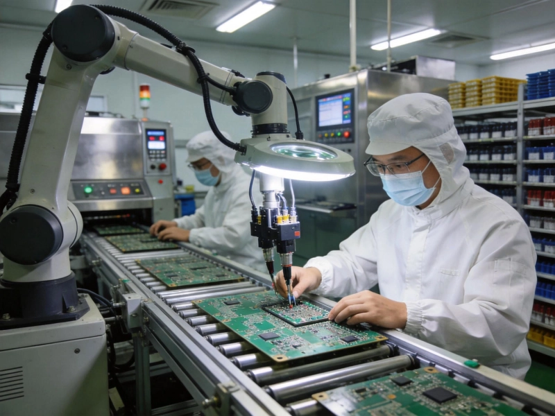
Testing, Quality, and Certifications
Capability isn't just about what they can make; it's about what they can verify. Does the spec sheet mention Automated Optical Inspection (AOI), X-Ray testing for BGA joints, or Electrical Flying Probe testing?
Equally important are their certifications. ISO9001 is standard, but if you are in automotive or medical, look for IATF16949 or ISO13485. These certifications prove the factory has systematic process controls in place, which is critical for maintaining consistency across large production runs.
Conclusion: Match Capability to Requirement
Decoding the Spec Sheet: Understanding a Factory's
Pcb Fabrication Capabilities ultimately comes down to alignment. Don't be dazzled by extreme specs if your application doesn't need them. Conversely, never compromise on critical parameters like thermal reliability or
Impedance Control just to save a few dollars.
Treat the spec sheet as a starting point for dialogue. Send your
Gerber Files early, ask for a free
Dfm analysis, and let the factory tell you which of their capabilities are actually necessary for your success.
Frequently Asked Questions
Q: What does 'High TG' mean on a PCB spec sheet?
A: It stands for High Glass Transition Temperature (typically ≥170°C). It indicates the board can withstand higher thermal stress during lead-free soldering without degrading or warping.
Q: Why is minimum line width/spacing important?
A: It determines the routing density. Tighter spacing allows for smaller components and denser designs but increases manufacturing complexity and cost.
Q: Should I always choose the factory with the highest specs?
A: No. Higher specs usually mean higher costs and longer lead times. Choose a factory whose capabilities perfectly match your design requirements to optimize both budget and time-to-market.