Open Nav

Standard 1oz copper PCBs simply can't handle the thermal and electrical demands of modern Power Electronics.
When your Pcb Design carries currents exceeding 20-30A, standard copper weights become inadequate. Heat buildup, voltage drop, and mechanical stress threaten reliability. This is where heavy copper PCBs step in, providing the current carrying capacity and Thermal Management that Power Electronics applications demand.
In this comprehensive guide, we'll explore what makes heavy copper PCBs unique, their capabilities, design considerations, and applications across power electronics industries.
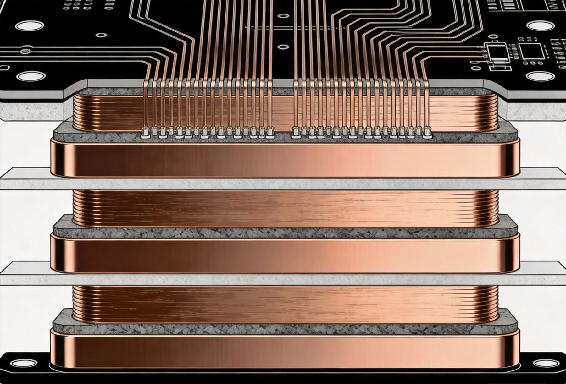
Heavy copper PCBs, also known as thick copper PCBs or extreme copper PCBs, use copper weights significantly heavier than standard PCB Fabrication. While standard PCBs typically use 1oz (35μm) or 2oz (70μm) copper, heavy copper boards range from 3oz (105μm) up to 20oz (700μm) or more.
Defining characteristics:
These boards aren't simply thicker copper versions of standard PCBs. The design considerations, manufacturing processes, and performance characteristics all differ significantly from conventional boards.
Understanding copper weight standards helps in selecting appropriate heavy copper PCBs:
These current capacities assume acceptable temperature rises and proper Thermal Management. Actual capacity depends on factors like PCB material, ambient temperature, and airflow.
Heavy copper PCBs deliver several key advantages for high-current applications:
The most obvious benefit is higher current capacity. Thicker copper reduces resistance, allowing more current flow without excessive heating. For applications handling 50-100A or more, heavy copper becomes necessary rather than optional.
Copper's thermal conductivity of 400 W/mK makes heavy copper PCBs excellent heat spreaders. Thick copper traces act as integrated heat sinks, moving heat away from hotspots and distributing it across the board. This reduces peak component temperatures and improves reliability.
Resistance drops proportionally with increased copper thickness. A 10oz copper trace has 1/10th the resistance of a 1oz trace. This reduces voltage drop across traces, improving efficiency and allowing tighter voltage regulation.
Heavy copper PCBs resist mechanical stress better than standard boards. The thicker copper provides:- Resistance to vibration and shock- Better resistance to thermal cycling stress- Enhanced durability in harsh environments
With better thermal management, heavy copper PCBs operate at lower temperatures for the same power dissipation. Lower temperatures directly correlate with longer component life and fewer failures.
Designing with heavy copper requires special considerations beyond standard Pcb Design:
While heavy copper allows narrower traces for given currents, proper sizing remains critical. Use IPC-2221 guidelines adjusted for heavy copper thicknesses:
Vias in heavy copper boards present unique challenges:- Standard via diameters become insufficient for high currents- Multiple parallel vias often needed for high-current paths- Via plating thickness increases for better current handling- Thermal vias connect heavy copper layers to enhance heat spreading
Design guidelines:
Heavy copper PCBs often use extensive copper pours for current distribution and thermal management:- Use large copper pours for power and ground planes- Connect pours with multiple vias between layers- Maintain adequate spacing between pours and signal traces- Consider split planes for different voltage levels
Heavy copper affects layer stackup design:- Heavy copper layers typically reserved for power distribution- Signal layers often use standard copper weights- Dielectric thickness increases to accommodate thick copper- Impedance Control becomes more challenging with thick copper
High-current components require special placement strategies:- Place power components close to each other to minimize trace lengths- Position sensitive components away from high-current areas- Consider thermal coupling between components- Allow adequate spacing for heat sink mounting
Manufacturing heavy copper PCBs requires specialized processes beyond standard PCB Fabrication:
Heavy copper boards start with thicker copper cladding:- Copper foil thickness selected based on requirements- Multiple layers of copper can be laminated for extreme thickness- Copper thickness consistency across the panel is critical
Etching thick copper presents unique challenges:- Longer etching times required- Risk of over-etching affecting trace dimensions- Tapered sidewalls common in heavy copper traces- Advanced etching processes needed for dimensional control
Drilling heavy copper boards requires:- Special drill bits for thick copper- Longer drilling times- Copper plating on via sidewalls must match thickness- Plasma desmear for better plating adhesion
Thick copper affects lamination:- Higher pressure required during lamination- Longer press cycles- Risk of resin flow issues- Careful control of lamination parameters essential
Heavy copper PCBs require additional quality checks:- Copper thickness verification across the board- Plated Through-hole quality inspection- Thermal performance testing- Current capacity verification
Heavy copper PCBs enable numerous power electronics applications:
Power supplies handling high currents rely on heavy copper PCBs:- Industrial power supplies (48V, 100V, 400V outputs)- DC-DC converters with high output currents- Battery chargers for electric vehicles- Solar panel inverters
Motor control applications benefit from heavy copper:- Industrial motor controllers- Electric vehicle motor drives- Robotics motor systems- HVAC system controllers
BMS applications require high current handling:- Electric vehicle battery packs- Energy storage systems- UPS battery systems- Industrial battery management
High-current applications in manufacturing:- Resistance welding equipment- Power tool controllers- Industrial heating systems- Plasma cutting equipment
Automotive applications demand heavy copper:- Electric powertrain controllers- DC-DC converters in vehicles- Battery charging systems- Power distribution units
Factory Automation relies on heavy copper PCBs:- PLC power modules- Servo drive controllers- High-current sensor interfaces- Industrial power distribution
Heavy copper PCBs come with cost considerations:
Despite higher costs, heavy copper can reduce overall design costs:- Eliminates need for separate heat sinks in some applications- Reduces component count by replacing discrete power resistors- Improves reliability, reducing warranty and replacement costs- Enables more compact designs
Heavy copper PCBs justify their cost when:- Currents exceed 30-50A continuously- Thermal management is critical- Reliability requirements are high- Total cost of ownership favors durability
Heavy copper PCBs compete with other high-current solutions:
Heavy copper PCB technology continues evolving:
Manufacturers now offer:- 30oz+ copper weights for extreme applications- Embedded copper cores for thermal management- Hybrid copper thicknesses on the same board
New substrate options enhance performance:- High-Tg materials for extreme temperature operation- Ceramic-filled substrates for improved thermal conductivity- Low-loss materials for high-frequency applications
Emerging technologies include:- Embedded liquid cooling channels- Integrated heat pipe connections- Phase-change material integration
Follow these guidelines for successful heavy copper designs:
Heavy copper PCBs aren't optional for high-current applications—they're essential. As power electronics push current handling to new limits, standard 1oz and 2oz PCBs simply can't meet requirements.
The benefits are clear: higher current capacity, superior thermal management, reduced voltage drop, and enhanced reliability. These advantages enable modern power electronics applications from electric vehicles to industrial Automation.
When designing power electronics requiring more than 30-50A per trace, heavy copper PCBs become the only viable solution. The investment in heavy copper technology pays dividends in performance, reliability, and total cost of ownership.
For engineers tackling high-current challenges, heavy copper PCBs provide the foundation for successful designs. Understanding their capabilities, design requirements, and manufacturing considerations ensures your power electronics projects succeed.
Ready to implement heavy copper PCBs in your power Electronics Design? Work with experienced PCB manufacturers who understand heavy copper requirements. Their expertise in fabrication, material selection, and design guidance can help you achieve optimal performance and reliability.
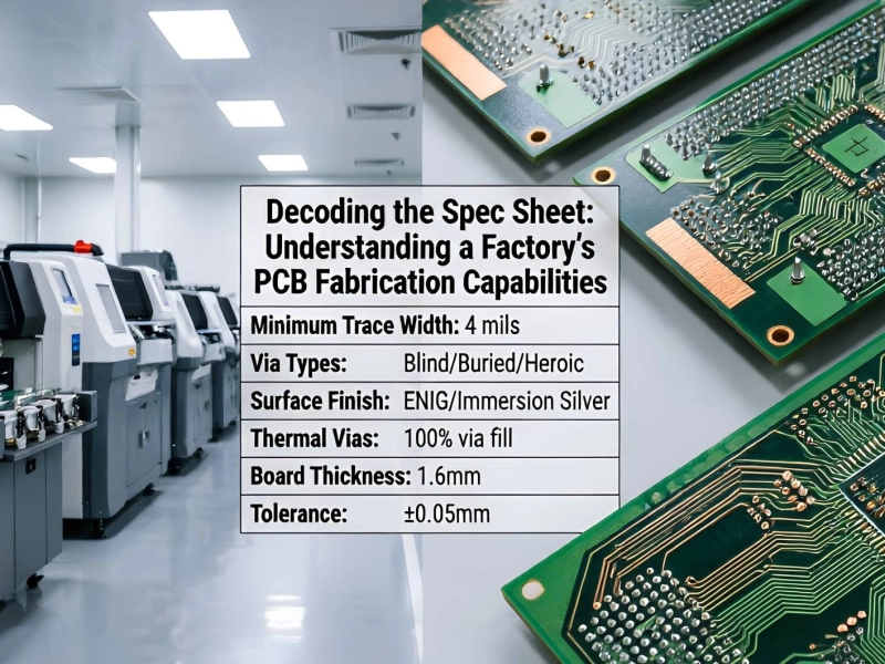
Decoding the Spec Sheet: Understanding a Factory's PCB Fabrication CapabilitiesJune/11/2026
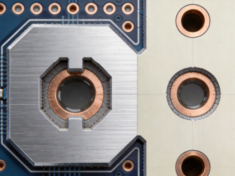
Back-drilling and Via-in-Pad: Advanced Capabilities for High-Speed DesignsSeptember/29/2026
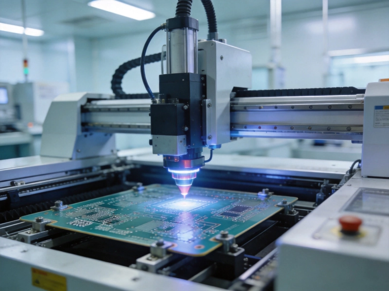
The Role of Equipment in Determining PCB Fabrication Capabilities (LDI, Laser Direct Imaging)September/09/2026
Why Global Brands Are Turning to PCB Fabrication in China in 2026May/21/2026
Minimum Trace and Space: How Far Has PCB Technology Advanced?July/01/2026
Any-Layer Interconnect: The Pinnacle of High-Density PCB TechnologyJuly/10/2026
Future-Proofing: Emerging Capabilities in the Next Generation of PCB MillsOctober/12/2026
Choosing the Right Assembly Partner: Capabilities, Capabilities, Certifications, and CapacitySeptember/28/2026