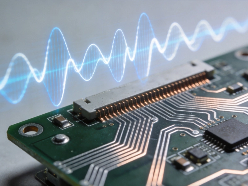
When designing printed circuit boards (PCBs) for power electronics, motor drivers, or high-performance computing, managing high current is one of the most critical challenges. Engineers frequently face a fundamental design decision: should they route power using traditional traces, or utilize expansive copper pours? While both methods conduct electricity, copper pour vs trace for high current is not merely an aesthetic choice; it dictates your board's thermal performance, electromagnetic compatibility (
Emc), and overall reliability.
Relying solely on traditional wide traces can quickly lead to routing bottlenecks and severe thermal hotspots. Conversely, poorly implemented copper pours can cause soldering issues or unintended EMI loops. Understanding how to strategically deploy both techniques is essential for robust hardware engineering.
 The Limitations of Traditional Traces in High-Current Paths
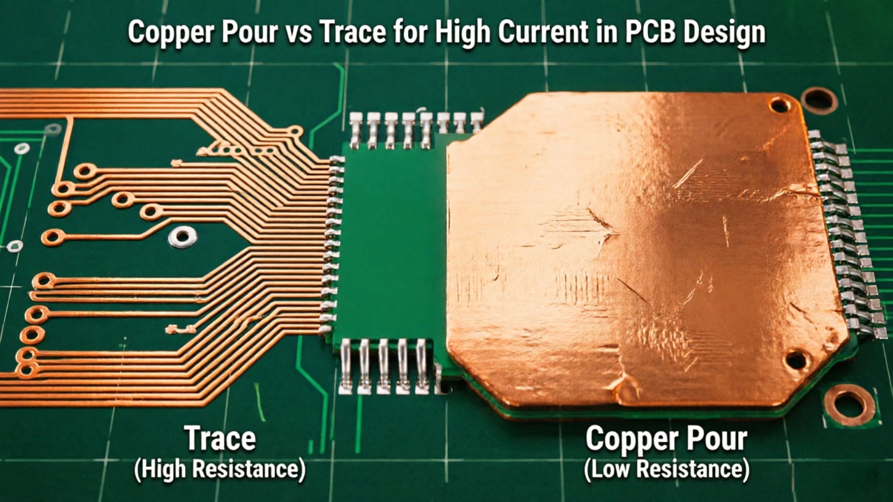
The most straightforward approach to carrying high current is simply making the trace wider. However, this method has strict physical limitations. According to IPC standards, pushing 20A or more through a standard 1oz copper layer requires an impractically wide trace—often exceeding 20mm. In dense, multi-layer boards, dedicating that much horizontal real estate to a single net is rarely feasible.
Beyond spatial constraints, wide traces suffer from current crowding at corners and vias, leading to localized heating. Furthermore, a single isolated trace provides a larger loop area for return currents, which acts as an antenna and increases electromagnetic interference (EMI).
The Strategic Advantages of Copper PoursCopper pours (or polygon fills) offer a superior solution for distributing high currents. By creating a massive cross-sectional area of copper, pours drastically reduce electrical resistance and IR voltage drops. But their benefits extend far beyond simple conductivity:
Solid vs. Hatched Fills: Making the Right ChoiceWhen configuring a copper pour, designers must choose between solid and hatched (mesh) fills. For high-current power delivery networks (PDN), solid copper pours are strictly recommended. Solid fills provide maximum cross-sectional area and lowest DC resistance. Hatched fills, while useful in high-frequency RF applications to reduce parasitic capacitance and prevent board warping, significantly reduce effective current-carrying capacity and increase thermal resistance. Using hatched fills for a 30A power path could result in unacceptable voltage drops and excessive heat generation.
Via Stitching: The Secret Weapon for Vertical Current FlowA common fatal flaw in high-current design is relying on a single via to transition power between layers. A standard 0.3mm via can safely carry only about 0.5A to 1A. To move 20A across layers, you need dozens of vias working in parallel.
This is where via stitching becomes mandatory. By placing arrays of stitching vias along high-current paths or directly beneath thermal pads, you create a robust three-dimensional copper structure. Via stitching minimizes vertical impedance, enhances heat transfer between inner and outer layers, and provides mechanical reinforcement. Always calculate the required number of parallel vias based on your target current and apply generous safety margins.
Practical Design Rules for High-Current LayoutsTo successfully integrate copper pours into your high-current design, follow these best practices:
ConclusionUltimately, the debate of copper pour vs trace for high current shouldn't be viewed as an either/or scenario. The most resilient PCB designs use thick, optimized traces for precise point-to-point connections, seamlessly transitioning into expansive solid copper pours for bulk power distribution and thermal spreading. By combining heavy copper weights, strategic via stitching, and intelligent
Dfm (
Design For Manufacturability) practices, engineers can safely deliver high currents while maintaining excellent
Signal Integrity and system reliability.