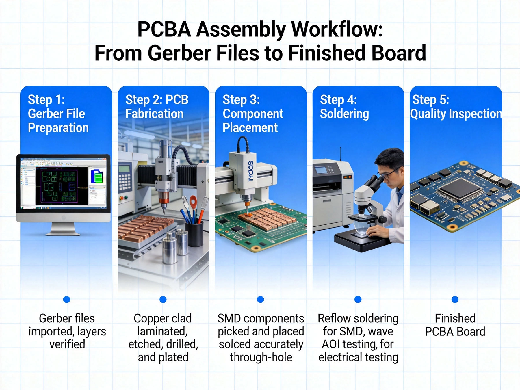
You've spent weeks perfecting your circuit board design. The schematics are complete, the layout is optimized, and you've exported your Gerber Files. Now what? How does your digital design transform into physical boards with components soldered in place and ready for your customers? Understanding the PCBA (PCB Assembly) workflow is essential whether you're a hardware startup founder, an engineer launching a new product, or someone just curious about how electronics come to life.
As someone who has worked with PCBA manufacturers across China for over a decade, I've seen countless projects succeed—and fail—based on how well stakeholders understand this critical workflow. The difference between a smooth delivery and a disaster often comes down to communication, documentation, and realistic expectations about the process.
In this comprehensive guide, we'll walk through every step of the PCBA workflow, from the moment you send your Gerber Files to when you receive your finished, assembled boards ready for product integration. By the end, you'll have the knowledge to navigate this process confidently and avoid common pitfalls that delay projects and drive up costs.
Before manufacturing can begin, you must provide a complete and accurate data package. Missing or incorrect files are the leading cause of delays in PCBA projects. Here's what you need:
Many EDA tools export these files automatically, but always verify completeness before sending. I've seen projects delayed for weeks because a designer forgot to include the drill file or exported coordinates in an unusual format the manufacturer couldn't interpret.
Once you submit your data package, the first thing a competent PCBA manufacturer does is perform a Dfm Review. This isn't just paperwork—it's a critical quality control step where experts examine your Design For Manufacturability issues that could cause problems during fabrication or assembly.
A thorough Dfm Review typically examines:
The DFM review is your chance to catch issues before they become expensive problems. A good manufacturer will provide specific recommendations for improvement. While you can choose to accept or reject each suggestion, ignoring critical DFM issues often leads to yield problems or field failures.
After DFM approval, your Gerber files undergo CAM (Computer-Aided Manufacturing) processing. This is where manufacturers translate your design data into the specific tools and processes they'll use to fabricate your boards.
CAM processing involves:
This step happens largely behind the scenes, but it's where many manufacturing problems originate. Errors in CAM processing can cause missing features, incorrect spacing, or other issues that manifest as defects in final boards.
With CAM work complete, the actual Pcb Fabrication begins. While the exact sequence varies by manufacturer and board complexity, the standard process includes:
Fabrication time varies from days to weeks depending on board complexity, layer count, and manufacturing workload. Simple double-sided boards might complete in 2-3 days, while complex multi-layer boards with controlled impedance and tight tolerances can take 2-3 weeks or more.
Throughout fabrication, various quality checks occur:
Quality issues caught during fabrication prevent problems downstream, but they also cause delays. Good manufacturers implement robust quality control to minimize yield loss and reduce rework.
While boards fabricate, manufacturers begin sourcing components based on your BOM. This step is where many projects experience unexpected delays. Component procurement challenges include:
The most common issues I've seen: incomplete part numbers that can't be verified, obsolete components that must be replaced, and second-sourcing decisions that take weeks to resolve. A complete, accurate BOM with verified manufacturer part numbers from the start dramatically reduces these problems.
PCBA manufacturers typically source components through multiple channels:
When purchasing from non-authorized sources, reputable manufacturers verify authenticity through visual inspection, X-ray inspection for counterfeits, and other methods. The counterfeit component problem is real, especially for popular microcontrollers and specialized ICs.
Sometimes the exact part you specified isn't available. Manufacturers may propose substitutions:
Always review proposed substitutions carefully. Some are perfectly acceptable, while others might affect performance, reliability, or software compatibility. The best manufacturers get approval before making changes that could impact your product.
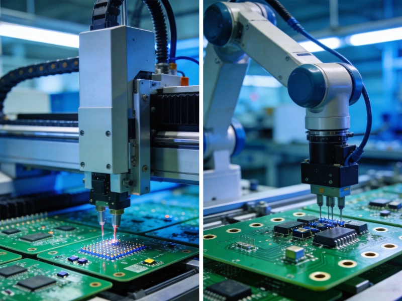
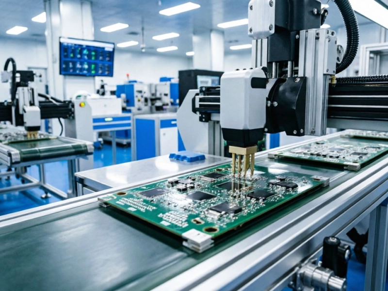
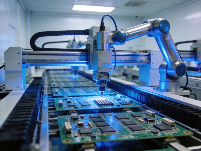
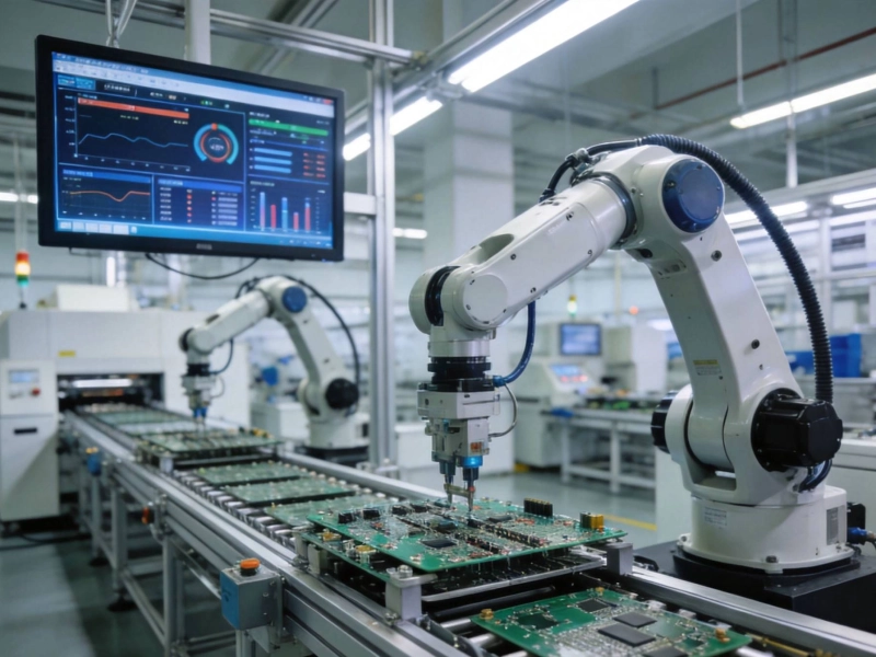
Surface Mount Technology (SMT) assembly is the most common and efficient method for populating modern PCBs. The standard SMT workflow includes:
Steel stencils are laser-cut or chemically etched with openings corresponding to solder pad locations. The stencil thickness and aperture size are carefully calculated based on component size and solder paste volume requirements. Precision here directly affects solder joint quality.
Solder paste—a mixture of solder powder and flux—is printed through the stencil onto the board. Modern solder paste printers use vision systems to align the stencil precisely to the board. The goal is depositing the correct amount of paste on each pad with consistent thickness across the panel. Too little paste causes opens; too much causes bridges or insufficient solder joint strength.
Pick-and-place machines suction components from reels, trays, or tubes and position them on the solder paste. Advanced placement machines achieve positioning accuracy of ±0.03mm or better, critical for fine-pitch components and BGAs. The coordinate file guides the machine, while vision systems verify correct component orientation before placement. High-speed placement machines can place tens of thousands of components per hour.
Boards pass through a reflow oven with carefully controlled temperature zones. The typical reflow profile includes:
Reprofile optimization is critical—too fast or too slow causes defects like tombstoning, solder balling, or insufficient wetting. Experienced manufacturers profile specifically for each product based on board size, component density, and thermal characteristics.
After reflow, automated inspection verifies solder joint quality:
While SMT dominates, some components must be through-hole for mechanical strength, thermal requirements, or simply because they're only available in through-hole packages. DIP (Dual In-line Package) assembly involves:
Wave soldering is highly efficient for through-hole components but requires careful process control to avoid bridging, insufficient solder, or thermal damage.
Many boards combine SMT and through-hole components. The typical sequence:
The challenge is protecting SMT components during wave soldering—hence the growing use of selective soldering for mixed-technology boards.
ICT uses a bed-of-nails fixture that makes electrical contact with specific test points on the board. This verifies:
ICT requires dedicated fixtures that match each board design, adding upfront cost but enabling high-volume testing efficiency.
While ICT verifies individual components and connections, functional testing verifies complete board operation:
Functional testing can range from simple power-up verification to complete application testing with test software and custom test fixtures.
For boards exposed to harsh environments, conformal coating provides protection against:
Coating materials include acrylics, silicones, urethanes, and epoxy, each with different characteristics. Application methods include spraying, dipping, or selective dispensing.
Solder flux residues can cause long-term reliability issues, especially in humid environments. Cleaning removes residues using:
Some modern no-clean fluxes claim to not require cleaning, but high-reliability applications often still specify cleaning.
Before packaging, final visual inspection verifies:
Boards must be properly protected for shipment:
Complete documentation typically includes:
Manufacturers typically offer various delivery methods:
The delivery method should be selected based on urgency, shipment size, and cost considerations.
Solution: Use automated BOM generation tools when possible. Verify every part number with component manufacturer datasheets before submission. Include complete manufacturer names and part numbers, not just descriptions.
Solution: Treat the DFM review as valuable feedback. Ask questions about recommendations you don't understand. Make informed decisions rather than blindly accepting or rejecting suggestions.
Solution: Understand typical lead times for your board complexity. Don't account for best-case scenario only. Build buffer time into your schedule for unexpected delays.
Solution: Clearly specify what testing you require. Provide test procedures, expected results, and acceptance criteria. Be specific about what constitutes a pass or fail.
Solution: Establish clear communication channels. Specify how and when you want updates. Respond promptly to manufacturer questions—delays often result from unanswered queries.
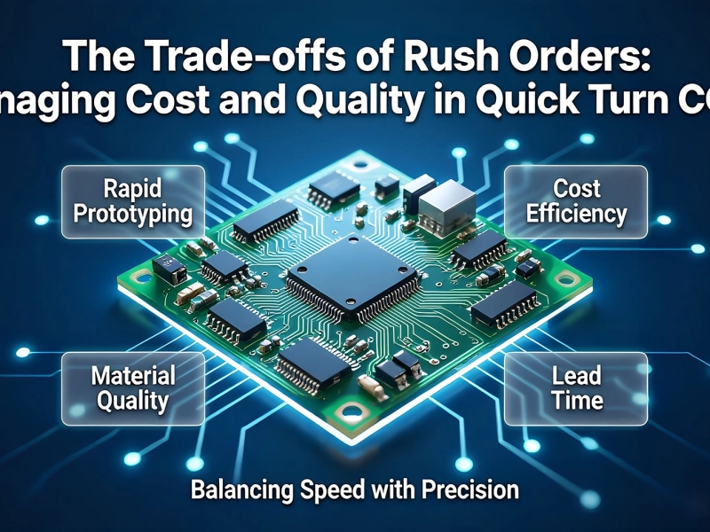
PCBA pricing depends on numerous factors:
Beyond the quoted price, consider:
The PCBA workflow from Gerber files to finished boards is a complex, multi-stage process involving numerous technical steps, specialized equipment, and skilled personnel. Understanding this workflow helps you set realistic expectations, communicate effectively with your manufacturing partner, and avoid common pitfalls that delay projects and drive up costs.
Whether you're bringing a product to market, scaling existing production, or simply need a few Prototype boards for development, the principles remain the same: provide complete and accurate data, maintain open communication, understand the manufacturing process, and choose a capable manufacturing partner.
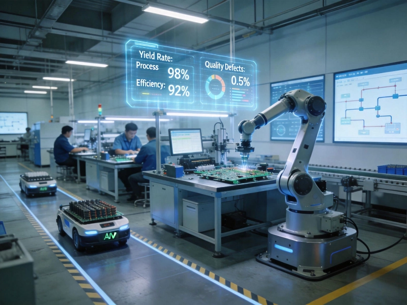
Electronics Manufacturing continues to evolve with Automation, AI-powered inspection, and digital systems improving efficiency and quality. However, the fundamentals of the PCBA workflow remain grounded in the process we've explored here. By understanding these fundamentals, you'll be better equipped to navigate the ever-changing landscape of Electronics Manufacturing.
Your Gerber files are just the beginning. The journey from digital design to physical product is complex, but with the right knowledge and partners, it's a journey you can navigate successfully.
You need Gerber files (RS-274X format including copper layers, solder mask, silkscreen, and drill data), a complete BOM with manufacturer part numbers, a coordinate (pick and place) file, and assembly drawings if you have special requirements. Complete, accurate documentation prevents delays.
Time varies significantly by board complexity and manufacturer workload. Simple Prototype boards might take 5-7 days total, while complex multi-layer boards with specialized components can take 3-4 weeks. Pcb Fabrication typically takes 2-7 days, component sourcing 3-10 days, and assembly 1-3 days.
PCB fabrication is just making the bare board without components. PCBA (PCB Assembly) includes fabrication plus component sourcing, assembly (soldering components to the board), testing, and final processing. PCBA provides complete, assembled boards ready to install in your product.
Work with manufacturers who source primarily from authorized distributors, verify components when sourcing from secondary markets, specify acceptable substitutions in your BOM, and consider implementing incoming component inspection for critical components. Reputable manufacturers have quality systems for component verification.
At minimum, require visual inspection (AOI) of solder joints and functional power-up testing. For higher volumes, ICT testing provides comprehensive verification. For BGAs and fine-pitch components, X-ray inspection is valuable. Define your testing requirements clearly in advance.
Yes, this is called "customer-supplied material" or "consignment assembly." However, manufacturers typically charge for handling customer components and won't be responsible for component quality. Most projects are more efficient when manufacturers source components themselves.
Contact your manufacturer immediately with clear documentation of the problems. Provide photos, test data, and descriptions. Good manufacturers will investigate root causes, implement corrective actions, and work with you to resolve issues quickly. Document everything for future prevention.
Managing Cost and Quality in Quick Turn PCBsJune/04/2026
SMT vs THT PCB Assembly in China: Which Technology is Right for Your Project?June/10/2026
How Chinese Manufacturers Ensure Precision in the SMT PCB Assembly ProcessJune/03/2026
The Benefits of Combining PCB Fabrication and AssemblyMay/22/2026
The Rise of Smart Factories: How Automation is Revolutionizing China's PCB SectorJune/16/2026
The Advantages of HDI PCB Fabrication for Compact ElectronicsMay/22/2026
The Economics of Customization: Balancing Performance and Budget in PCB DesignJune/17/2026
Top Trends Shaping the Chinese PCB Manufacturing Industry in 2026May/21/2026