Open Nav

Every printed circuit board starts as a blank sheet of copper clad laminate. A thin layer of copper, typically 18 to 70 microns thick, covers an insulating substrate made of fiberglass and epoxy resin. Transforming this blank canvas into the intricate network of conductive traces that carry signals and power across modern electronics requires a process called etching. It is the fundamental manufacturing step that defines the shape of every circuit path, every pad, every via, and every ground plane on the board.
Understanding how etching works gives insight into why certain design choices matter. Trace widths, spacing, and copper thickness are not arbitrary. They are constrained by the realities of the etching process. Engineers who understand these constraints can design boards that manufacture reliably and perform predictably.
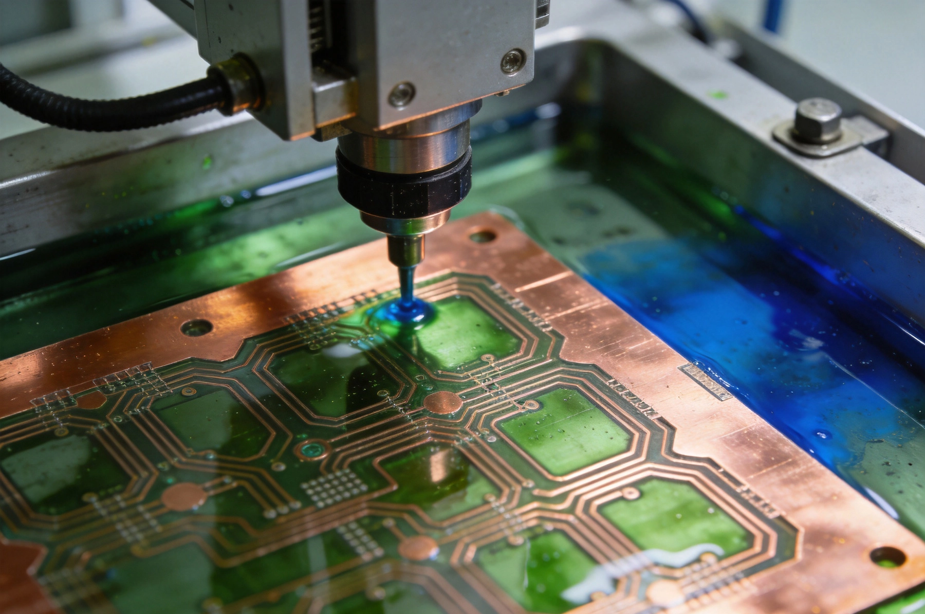
Etching is a subtractive process. The manufacturer starts with copper everywhere and selectively removes the copper that is not wanted, leaving behind only the desired circuit pattern. The key to this selectivity is a protective layer called photoresist. Photoresist is a light-sensitive polymer that, when exposed to ultraviolet light through a photographic mask, undergoes chemical changes that make it either soluble or insoluble in developer solution.
There are two types of photoresist. Positive photoresist becomes soluble where exposed to light, so the exposed areas wash away during development, leaving resist only in the unexposed areas. Negative photoresist behaves oppositely, becoming insoluble where exposed, so the unexposed areas wash away. Pcb Manufacturing predominantly uses negative photoresist because it offers better adhesion to copper and better chemical resistance during the etching step.
Wet etching is the most common method for creating circuit boards, accounting for the vast majority of production worldwide. The process follows a carefully choreographed sequence of chemical and mechanical steps.
Before applying photoresist, the copper surface must be perfectly clean. Any oxidation, contamination, or residue will prevent proper resist adhesion, leading to defects called lifting or undercutting where the resist peels away during etching. The cleaning process typically involves microetching with a mild acid solution to remove surface oxides, followed by rinsing and drying. Some processes also include a chemical treatment to micro-roughen the copper surface, creating microscopic pits that improve resist mechanical bonding.
The cleaned laminate enters a coating machine where liquid photoresist is applied. This can be done by roller coating, curtain coating, or electrophoretic deposition. Roller coating passes the board between rollers that spread a thin, uniform layer of resist across the surface. Curtain coating creates a falling curtain of resist through which the board passes. Electrophoretic deposition uses an electric field to deposit resist ions onto the copper surface, offering excellent uniformity and coverage of irregular surfaces.
The applied resist is then soft-baked to drive off solvents and harden the coating enough to handle, but not so much that it cannot be exposed and developed. Typical soft bake temperatures range from 70 to 90 degrees Celsius for 10 to 20 minutes.
A phototool, also called a film or mask, carries the circuit pattern as a transparency with opaque and clear areas. The phototool is aligned precisely over the resist-coated board in an exposure machine. High-intensity ultraviolet light shines through the phototool, exposing the resist in the pattern of the clear areas on the mask.
For negative photoresist, the exposed areas polymerize and become insoluble. The unexposed areas remain soluble. Exposure energy must be carefully controlled. Underexposure leaves the resist incompletely polymerized, causing it to wash away partially during development. Overexposure can cause light scattering that exposes areas that should remain protected, leading to line width loss.
The exposed board enters a developer bath, typically an aqueous solution of sodium carbonate or potassium carbonate for negative resist. The unexposed resist dissolves away, revealing the copper underneath in the areas that will become the spaces between traces. The exposed resist remains, protecting the copper that will become the circuit traces.
Development time and temperature are critical parameters. Insufficient development leaves resist residue in the spaces, which will block etching and create shorts. Excessive development can attack the edges of the exposed resist, causing line width reduction and poor edge definition.
With the photoresist defining the circuit pattern, the board enters the etching machine. Etchant chemistry removes the exposed copper while leaving the resist-protected copper untouched. The most common etchant for printed circuit boards is cupric chloride, though ferric chloride and alkaline ammonia-based etchants are also used.
Cupric chloride etching works by oxidizing metallic copper to cupric ions in solution. The reaction proceeds as copper metal reacts with cupric chloride to form cuprous chloride, which is then reoxidized back to cupric chloride by bubbling air or adding oxidizers through the solution. This makes cupric chloride a regenerative etchant that can be used continuously with proper maintenance.
The etching process is not instantaneous. Copper must be removed not just vertically through the thickness of the foil, but also horizontally under the resist edges. This horizontal etching, called undercut, is unavoidable but can be minimized through process control. Typical undercut for a standard etching process might be 0.5 to 1.0 mils per side, meaning a trace designed as 8 mils wide might emerge as 6 to 7 mils after etching.
After etching removes the unwanted copper, the remaining photoresist must be stripped away to reveal the finished copper traces. Alkaline strippers dissolve the resist without attacking the copper. The stripped board is rinsed, dried, and inspected. Any remaining resist would interfere with subsequent processes like Solder Mask application or surface finishing.
While wet etching dominates Pcb Manufacturing, dry etching methods exist for specialized applications. Plasma etching uses ionized gas to physically sputter or chemically react with copper, removing it without liquid chemicals. Reactive ion etching combines physical sputtering with chemical reaction for highly anisotropic etching profiles with minimal undercut.
These dry methods offer better control over etching profiles and can achieve finer feature sizes than wet etching. However, the equipment is significantly more expensive and the throughput is lower. Dry etching finds use in semiconductor manufacturing and for very High-density Interconnect boards where trace widths below 2 mils are required.
The composition of the etching solution directly affects etch rate and uniformity. Cupric chloride concentration, free acid content, and temperature all influence how quickly copper dissolves. Operating outside the recommended ranges leads to problems. Too weak an etchant etches slowly, increasing production time and potentially causing over-etching before completion. Too strong an etchant attacks the resist and causes excessive undercut.
Etchant chemistry is monitored through regular analysis and adjusted by adding fresh chemicals or regenerating spent etchant. Automated dosing systems maintain concentration within tight tolerances for consistent results.
Static etching, where boards simply sit in etchant solution, produces poor results. Fresh etchant must continuously reach the copper surface while dissolved copper must be carried away. Agitation through mechanical movement, air bubbling, or spray nozzles accomplishes this mixing.
Spray etching machines use arrays of nozzles to spray fresh etchant onto the board surface at controlled pressure. Higher spray pressure improves etch rate but can cause resist damage on fine features. Lower pressure is gentler but slower. Finding the right balance for the specific board design is part of process engineering.
Thicker copper takes longer to etch completely through. A standard 1 ounce copper foil, about 35 microns thick, might etch in 60 to 90 seconds under typical conditions. Heavy copper at 3 or 4 ounces, over 100 microns thick, might require 3 to 5 minutes. Longer etch times increase undercut, which is one reason why heavy copper designs require wider trace widths and spacing to achieve the same final dimensions after etching.
Etch rate increases with temperature, roughly doubling for every 10 degrees Celsius rise within the operating range. However, excessive temperature degrades photoresist, causes excessive undercut, and creates safety hazards with volatile etchant components. Most wet etching processes run at 40 to 50 degrees Celsius, balancing speed against quality.
The Minimum Trace Width and spacing a manufacturer can reliably produce depends on their etching capabilities. Standard processes handle 4 mil traces and spaces. Advanced processes can achieve 2 mils or less. These numbers account for the undercut that occurs during etching. A designer specifying 4 mil traces might be told that the etching process requires starting with 5 or 6 mil traces to end up at 4 mils after undercut.
When mixing trace widths on the same board, avoid abrupt transitions from very wide to very narrow traces in adjacent areas. The etching dynamics differ for wide copper areas versus narrow traces, potentially causing over-etching of narrow traces while wide areas are still etching. Adding dummy copper patterns or thieving patterns in sparse areas helps balance copper distribution and improves etching uniformity.
The ratio of copper thickness to trace width, called the aspect ratio, affects etching quality. High aspect ratios, where thick copper forms narrow traces, are difficult to etch cleanly. The etchant has trouble penetrating the narrow channel between resist walls to reach the bottom of the copper, leading to incomplete etching at the trace base while the tops etch completely. For heavy copper designs, wider traces are necessary to maintain manufacturable aspect ratios.
After etching, boards undergo inspection to verify that the circuit pattern matches the design. Automated optical inspection systems scan the board surface, comparing the etched pattern against the design database to detect opens, shorts, and dimensional errors. Critical dimensions are measured using optical microscopes or coordinate measuring machines.
Cross-sectional analysis cuts samples from production panels and examines them under a microscope to verify etch profiles and measure undercut. This destructive testing validates that the etching process is producing the intended trace geometry.
Etching chemicals are hazardous. Cupric chloride is corrosive and toxic. Spent etchant contains dissolved copper that cannot be discharged to wastewater without treatment. Modern PCB facilities employ sophisticated waste treatment systems that neutralize acids, precipitate heavy metals, and recover copper for recycling.
Worker safety requires proper ventilation, personal protective equipment, and training in handling chemicals. Automated etching machines reduce human exposure by containing the process within closed systems. Environmental regulations in most jurisdictions strictly control etchant handling, storage, and disposal.
Etching is the transformative step that turns raw copper clad laminate into functional circuit boards. The process combines photochemical patterning with chemical removal to create conductive pathways with precision measured in thousandths of an inch. Understanding how etching works, what affects its quality, and how to design for it allows engineers to create PCBs that manufacture reliably and perform as intended.
From the surface preparation that ensures resist adhesion to the final strip that reveals finished traces, each step in the etching sequence contributes to the outcome. Chemistry, temperature, agitation, and time must all be controlled within tight windows. When they are, the result is the precise circuit pattern that makes modern electronics possible.
Cupric chloride is the most widely used etchant for PCB manufacturing due to its regenerative properties, consistent etch rates, and relatively straightforward process control. It can be continuously regenerated by oxidation, making it economical for high-volume production. Ferric chloride is also common, especially in smaller shops, though it requires more careful waste handling.
Standard wet etching typically produces 0.5 to 1.0 mils of undercut per side. This means a trace will be narrower than the photoresist opening by 1 to 2 mils total. Designers should account for this when specifying trace widths. Advanced etching processes with better spray control can achieve undercut below 0.5 mils per side.
While the same basic chemistry works for different copper weights, process parameters must be adjusted. Heavy copper requires longer etch times, which increases undercut. This is why heavy copper designs need wider trace widths to achieve the same final dimensions. Some manufacturers use specialized equipment or multiple etching stages for very heavy copper boards.
Uneven etching can result from poor resist adhesion, inconsistent spray pressure, temperature gradients in the etching bath, or uneven copper distribution across the board. Adding copper thieving patterns in sparse areas helps balance copper loading and improves etching uniformity. Proper cleaning and surface preparation before resist application is essential for even etching.
Dry etching offers better control and can achieve finer features, but it is slower and more expensive than wet etching. For most PCB applications, wet etching provides the best balance of quality, speed, and cost. Dry etching is reserved for specialized applications requiring sub-2 mil features or vertical sidewall profiles that wet etching cannot achieve.
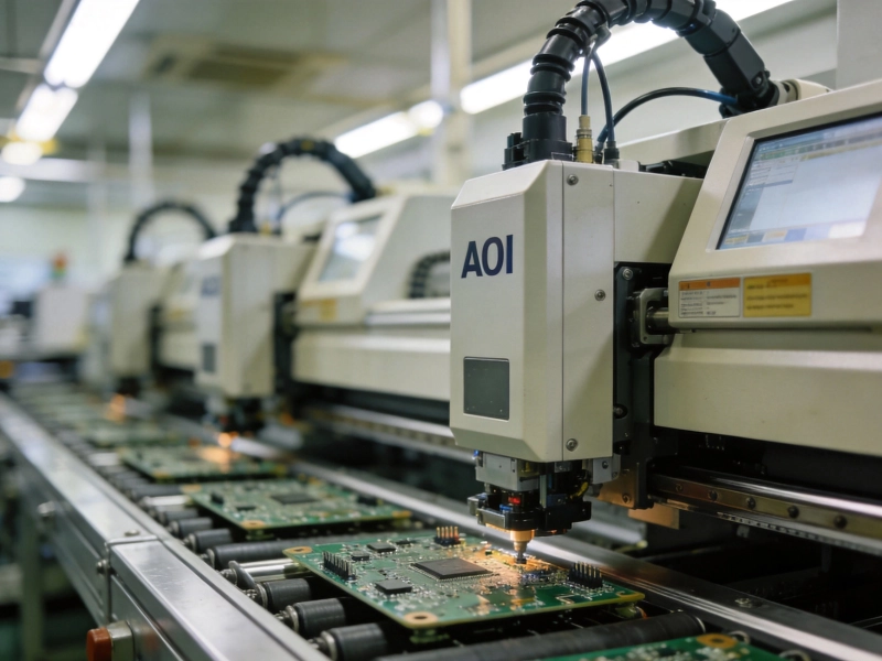
Quality Control 101: AOI, X-Ray, and Electrical Testing in PCB ProductionAugust/10/2026
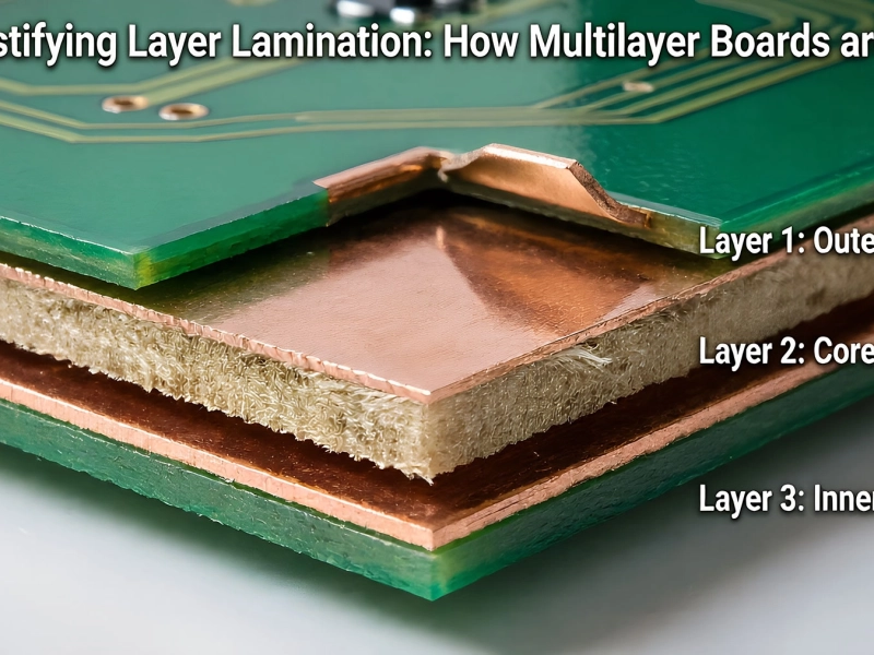
Demystifying Layer Lamination: How Multilayer Boards are BuiltJune/05/2026
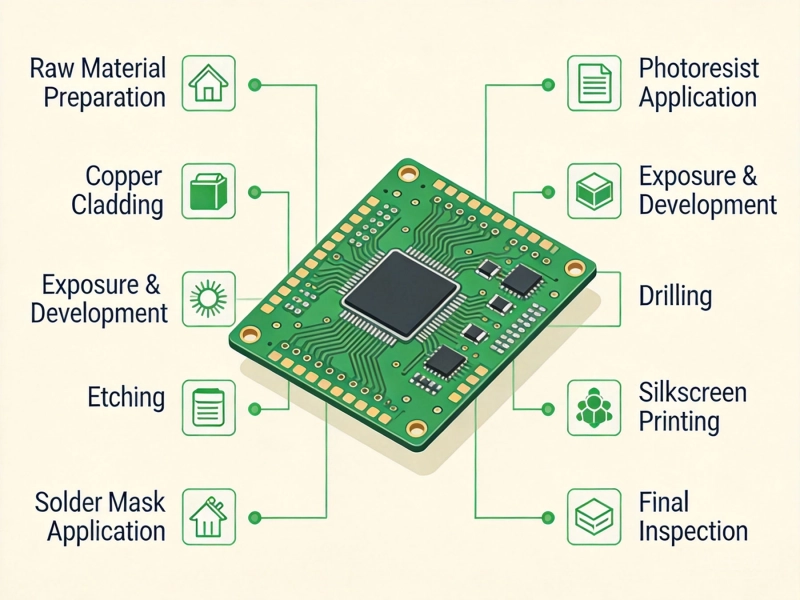
A Step-by-Step Walkthrough of the PCB Fabrication ProcessMay/21/2026
Solder Mask and Silkscreen: More Than Just Aesthetics in the PCB ProcessJuly/20/2026
Understanding Copper Plating: Ensuring Connectivity and Durability in PCBsJuly/09/2026
E-Commerce vs. Traditional Sales: How Buying PCB Services Has ChangedJuly/25/2026

The Chemistry of PCB Cleaning: Why Ionic Contamination MattersSeptember/04/2026
Is PCB Fabrication in China Still the Most Cost-Effective Option? A 2026 AnalysisJuly/27/2026