
Ask most engineers what solder mask and silkscreen do on a PCB, and you'll get answers focused on appearance. Green boards look professional. White silkscreen makes components readable. These are true observations, but they completely undersell the functional importance of these two process steps.
In reality, solder mask and silkscreen are among the most consequential finishing processes in Pcb Manufacturing. The mask layer prevents solder bridges during assembly. The silkscreen enables accurate component placement and field serviceability. Getting either wrong produces boards that might look fine but fail repeatedly in production or the field.
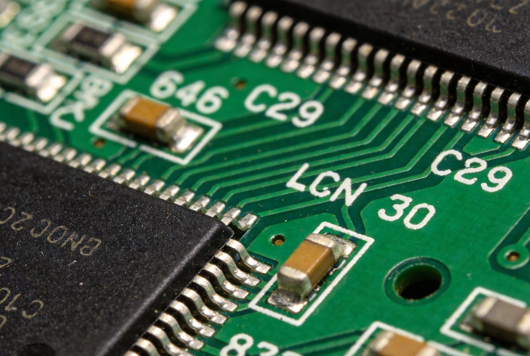
Solder mask exists to control where solder goes during assembly. Without it, molten solder would wick unpredictably across every exposed copper surface, creating bridges between adjacent pads, traces, and vias. In Surface Mount assemblies with fine pitch components—0.5mm or 0.4mm pitch QFNs and BGAs—uncontrolled solder flow would make assembly nearly impossible.
The mask covers the dielectric surfaces while leaving pads, holes, and specific features exposed for soldering. The accuracy of this coverage determines whether your assembly process produces reliable joints or a field of solder bridges requiring expensive rework.
Modern solder mask application uses photoimageable inks that expose and develop like a photographic process. The board gets coated with liquid mask or dry film, then a phototool defines which areas remain and which get removed to expose pads. This process achieves feature tolerances of 50-100 microns, sufficient for most commercial electronics.
Liquid photoimageable (LPI) mask dominates current Pcb Manufacturing. It's applied as a spray or curtain coat, then UV-cured through a phototool to create the final pattern. LPI masks offer excellent resolution, good chemical resistance, and reasonable flexibility for boards that need to flex during use.
Dry film mask comes in sheet form and laminates onto the board surface. It provides outstanding thickness control and consistent coverage, but works best on flat surfaces without deep cavities or components already mounted. Military and aerospace applications often specify dry film for its consistency and documented process controls.
The color of your solder mask isn't cosmetic trivia. Different pigments absorb and reflect heat differently during reflow, affecting temperature profiling. Darker masks—green, black, blue—absorb more radiant heat, while lighter masks—yellow, red, white—reflect more. Your assembly engineer needs to account for mask color when developing the reflow profile, particularly for boards with mixed component thermal masses.
The relationship between pad size and mask opening determines assembly yield. Too much mask overlapping the pad reduces the available solderable area, potentially creating weak joints or incomplete wetting. Too little mask opening leaves copper exposed too close to adjacent features, increasing bridge risk.
Standard practice specifies mask openings 2-4 mils larger than the underlying pad on each side. For a 60-mil square QFN pad, this means a 64-68 mil mask opening. The specific value depends on the fabricator's process capability and the density of surrounding features.
Fabricators routinely adjust mask openings based on their process capabilities and the specific design geometry. A well-designed board leaves room for these adjustments. A cramped layout with features packed too tightly forces the fabricator to choose between inadequate mask openings or bridging risk—neither option serves your assembly goals.
Vias present a special case for solder mask. An open via allows solder to wick through the barrel during assembly, potentially causing voids in nearby joints or creating solder splatter on the board underside. Tenting covers the via with mask material, sealing it from the assembly process.
Tented vias work for most applications—the mask bridges across the via opening and stays intact through assembly reflow. For boards that need guaranteed sealing, via plugging fills the barrel with mask material before tenting, providing redundant protection against solder intrusion.
Blind and Buried Vias often require tenting or plugging to prevent solder from wicking into internal layer connections during assembly. Without proper via treatment, the thermal mass of solder inside a via barrel can cause downstream assembly problems or create thermal imbalance during operation.
Thermal vias under heat spreaders deserve special consideration. Tenting thermal vias under a BGA heat spreader prevents solder from flowing into the barrel, but the mask material itself becomes part of the thermal path. Some designers prefer leaving these vias open or using conductive fill to maximize thermal conductivity, accepting the assembly risk that solder intrusion might create.
Silkscreen—the white or light-colored markings printed on the PCB surface—serves functions that extend far beyond aesthetics. The primary purpose is component identification. Reference designators, polarity marks, pin-one indicators, and orientation dots enable accurate placement during assembly and allow technicians to locate specific components during testing and repair.
During assembly, machines place components based on pick-and-place data linked to the CAD files, not the silkscreen markings. The human-visible markings matter for manual assembly steps, Prototype verification, and any situation where visual confirmation adds confidence. For boards that will ever be touched by human hands—during debug, repair, or field service—silkscreen provides essential orientation information.
Silkscreen also carries manufacturing information that aids production and quality processes. Board part numbers, revision codes, lot numbers, and date codes help trace assemblies through manufacturing and support warranty service. When a field failure occurs, the silkscreen markings allow identification of the specific board version without consulting documentation.
Silkscreen printing achieves significantly lower resolution than solder mask. Standard screen printing produces features down to about 5-6 mils line width, which sounds adequate until you try to print tiny reference designators next to fine-pitch components. A 0402 resistor needs a reference designator smaller than the component itself, and the resulting text may be barely legible without magnification.
For high-density boards, some fabricators offer legend printing using direct legend (DL) processes—essentially printing silkscreen using a photoprocess similar to mask application. DL achieves 2-3 mil resolution, making tiny text actually readable. The tradeoff is higher cost and potentially reduced durability compared to traditional screen-printed legend.
Board flex can crack silkscreen ink over thermal cycles. If your design requires flexible operation, specify flexible-rated legend inks that maintain adhesion through repeated flexing. Standard inks on flex circuits often develop cracks along the substrate bends, rendering text illegible and potentially flaking particles into the assembly.
Silkscreen prints on top of solder mask. This means the mask surface properties directly affect legend adhesion and durability. Some mask formulations—with particular surface energies or post-curing treatments—don't bond well with standard legend inks. The result is legends that scratch off easily or delaminate during thermal cycling.
Ask your fabricator about their mask and legend process compatibility. Reputable manufacturers test their mask/legend combinations to ensure reliable adhesion. When you change mask suppliers or formulations, re-validate legend adhesion rather than assuming existing processes will transfer.
Mask color also affects silkscreen contrast. White legend on green mask provides excellent contrast. White legend on white mask is essentially invisible. Light yellow legend on yellow mask barely passes readability requirements. If your brand demands specific mask colors, verify that legend contrast remains adequate for practical use.
Boards destined for harsh environments—automotive under-hood, industrial control, outdoor enclosures—require special consideration for both mask and legend durability. Standard materials may degrade prematurely under thermal cycling, chemical exposure, or UV radiation.
High-reliability mask formulations resist the specific environmental stressors your application imposes. Automotive specs often require mask materials tested for specific temperature ranges, thermal shock resistance, and resistance to automotive fluids. Specify materials that meet the relevant environmental standard rather than assuming commercial-grade materials will survive.
Legend inks for harsh environments similarly require qualification. Standard epoxy-based inks may chalk, crack, or fade under UV exposure. Polyimide-based or UV-cured inks provide improved durability at higher cost. For applications where silkscreen legibility must survive decades of field service, the additional material cost is trivial compared to the cost of service calls to identify obscure components.
Design decisions made long before fabrication determine how well your boards survive mask and legend processing. Keep silkscreen features away from pad edges—at least 5 mils clearance prevents mask overlap that can cause ink to wick onto solderable surfaces. Overlapping silkscreen on pads creates Solderability problems that are difficult to diagnose and resolve.
Provide adequate silkscreen text sizing. Minimum character height of 35 mils maintains readability for most applications. Below 25 mils, text becomes difficult to read without magnification, defeating the purpose of component identification. If your board density forces tiny text, consider using direct legend or adding a separate silkscreen layer for critical markings.
Avoid placing silkscreen over ground planes without thermal relief. The ink doesn't adhere well to bare copper, and the trapped air can cause bubbling during curing. Route silkscreen traces around plane areas or specify dielectric-backed silkscreen routing that maintains clearance from exposed copper.
Mask voids—small areas where mask coverage is incomplete—create reliability risks that are difficult to detect. A void over a thin trace creates an unintentional exposed copper surface that can corrode over time or create leakage paths for high-impedance circuits. Automated optical inspection catches most voids, but the smallest ones slip through and cause field failures.
Mask adhesion failure shows up as bubbling, peeling, or delamination. Root causes include surface contamination before masking, improper cure, or thermal mismatch between mask and substrate. Adhesion failures often manifest after assembly reflow, when the thermal stress of the assembly process overcomes marginal mask bonding.
Silkscreen misalignment causes component designators to appear in the wrong locations, making assembly documentation misleading rather than helpful. This defect usually results from artwork registration errors in the fabrication process. Check silk alignment during incoming inspection before populating boards—you can't trust your assembly documentation if the silkscreen doesn't match the actual component positions.
Automated optical inspection (Aoi) catches most solder mask defects, but standard Aoi resolution may miss small voids or mask anomalies under dense component footprints. For high-reliability applications, request additional inspection methods—laser scanning or X-ray Inspection can reveal problems hiding under BGAs and other area-array packages.
Silkscreen legibility inspection is largely visual but benefits from documented criteria. Specify minimum character height, stroke width, and contrast ratios in your quality requirements. Without explicit standards, fabricators may deliver boards that meet their internal specifications but fail your practical readability needs.
Accelerated testing for harsh environment applications validates mask and legend durability. Thermal cycling, humidity exposure, and UV aging tests reveal whether your material choices survive expected service conditions. Don't assume commercial-grade materials are adequate—test them under realistic conditions to establish confidence in long-term performance.
Solder mask and silkscreen aren't decorative finishing steps—they're functional coatings that directly affect assembly yield, product reliability, and serviceability. Solder mask controls solder flow during assembly and protects copper traces from environmental exposure throughout the product's life. Silkscreen enables accurate assembly, supports field service, and carries identification information that outlasts documentation.
Design decisions about mask color, via treatment, legend resolution, and environmental ratings shape manufacturing outcomes long before boards reach assembly. Taking these process steps seriously—specifying them clearly, validating them appropriately, and accounting for their limitations—produces boards that assemble cleanly and perform reliably.
The aesthetic dimension isn't entirely absent from the picture. Boards that look professionally finished inspire confidence in your products and your company's attention to detail. But that's a side benefit. The real value of proper solder mask and silkscreen processing is the invisible contribution it makes to every reliable joint, every trace that survives thermal cycling, and every component that gets placed correctly the first time.
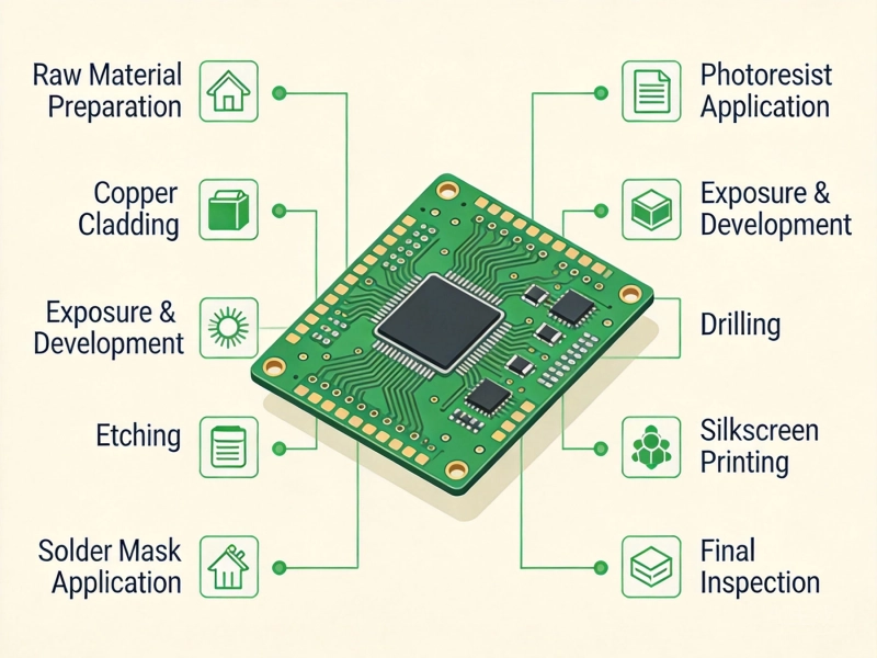
A Step-by-Step Walkthrough of the PCB Fabrication ProcessMay/21/2026

Is PCB Fabrication in China Still the Most Cost-Effective Option? A 2026 AnalysisJuly/27/2026
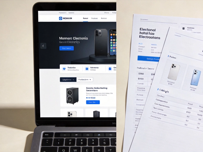
E-Commerce vs. Traditional Sales: How Buying PCB Services Has ChangedJuly/25/2026

Understanding Copper Plating: Ensuring Connectivity and Durability in PCBsJuly/09/2026
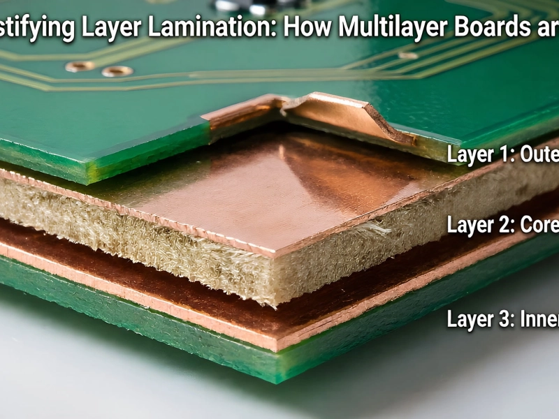
Demystifying Layer Lamination: How Multilayer Boards are BuiltJune/05/2026
Etching Explained: How Circuit Patterns are Precisely Formed on Copper Clad LaminatesJuly/30/2026

The Chemistry of PCB Cleaning: Why Ionic Contamination MattersSeptember/04/2026

How Automation is Revolutionizing China's PCB SectorJune/03/2026