Open Nav

Every PCB that ships to customers should work correctly the first time. Achieving this goal requires systematic Quality Control at every production stage. Three complementary inspection technologies form the backbone of modern Pcb Quality Assurance: Automated Optical Inspection (Aoi), X-ray Inspection, and electrical testing. Each method addresses different defect types and production stages, creating a comprehensive quality net when properly combined.
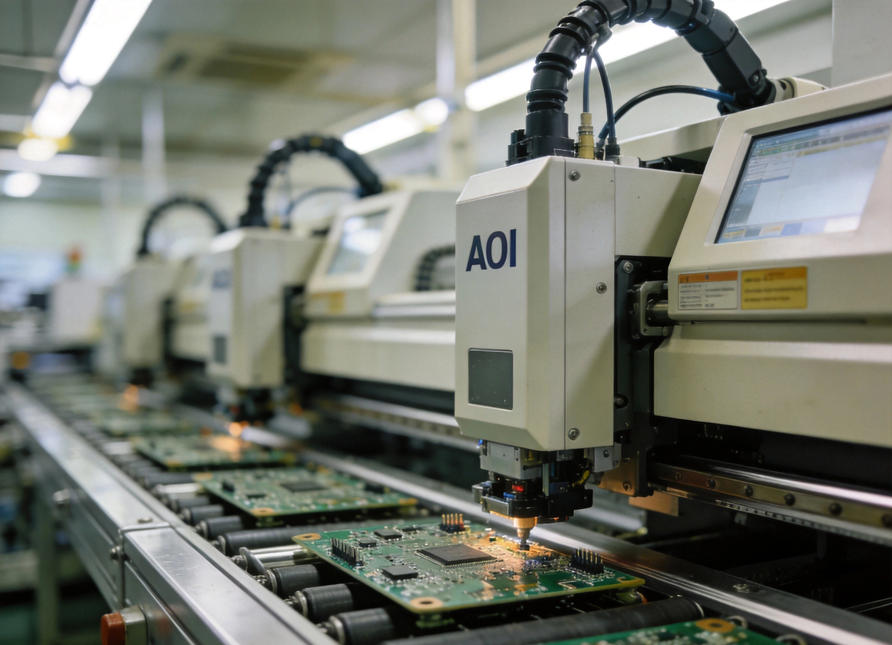
PCB defects fall into several categories, each requiring specific detection methods. Assembly defects include misplaced components, tombstoned parts, insufficient or excess solder, bridging between pads, and cold solder joints. Fabrications defects involve open circuits, short circuits, tracewidth violations, and dielectric problems. Both categories can cause field failures if not caught during production.
The cost of finding defects increases dramatically as boards progress through assembly and into customer hands. Catching problems during inline inspection costs pennies. Reworking completed boards costs dollars. Field failures cost reputation and relationships. Effective Quality Control programs prioritize early detection while maintaining final verification.
Industry standards like Ipc-a-610 define acceptance criteria for electronic assemblies, establishing baseline quality expectations. Understanding these standards helps buyers specify appropriate quality levels and inspection requirements for their applications.
Automated Optical Inspection uses cameras and image processing software to examine boards at various production stages. Aoi systems compare captured images against known-good reference data, flagging deviations for operator review. Modern AOI achieves inspection rates compatible with production line speeds while maintaining consistent detection sensitivity.
AOI cameras capture images of board surfaces at multiple angles and lighting conditions. Structured lighting patterns reveal surface elevation differences that indicate component presence, position, and orientation. Image processing algorithms compare captured data against golden board references or CAD data.
Systems typically operate in teach mode where operators define acceptance criteria using known-good samples, or comparison mode where boards compare against CAD data directly. Both approaches have advantages depending on board complexity and volume requirements.
Resolution determines detection capability. Systems designed for 0402 components might miss defects on fine-pitch devices. Match AOI capabilities to your smallest component packages for comprehensive coverage.
Post-solder paste printing inspection verifies stencil application quality before components place. Detecting insufficient paste early prevents downstream rework. This stage catches approximately 60% of assembly defects according to industry studies.
Post-placement inspection confirms components landed correctly before reflow. Missing parts, rotated components, and shifted placements get caught before irreversible solder attachment. Some systems measure coplanarity of Gull-wing leads.
Post-reflow inspection examines completed solder joints for defects like bridging, insufficient solder, Solder balls, and component issues like tombstones or shifted parts. This represents the primary AOI inspection point for most assemblies.
Final inspection might combine AOI with visual verification for cosmetic defects, labeling accuracy, and assembly completeness.
AOI excels at detecting visible defects including missing components, wrong polarity parts, shifted placements, bridging, insufficient solder, and tombstoning. Systems provide fast feedback enabling statistical process control and rapid corrective action.
However, AOI cannot see beneath components. Hidden solder joints under BGA packages, QFN devices, and leadless components escape optical detection. Board defects like delamination, internal shorts, and trace problems require other methods. AOI also struggles with components under other parts, creating blind spots in dense assemblies.
X-ray Inspection penetrates component bodies to reveal internal features invisible to optical systems. This capability makes X-ray essential for verifying hidden solder connections that AOI cannot inspect.
X-ray systems generate radiation that passes through materials, with attenuation varying by material density and atomic number. Copper appears brighter than surrounding substrate, while solder shows distinctly from component bodies and Pcb Materials. Imaging sensors capture transmission patterns, creating visual representations of internal structures.
2D X-ray provides plan-view images showing component positions, ball presence, and gross defects. This works well for BGA void measurement and basic bridge detection.
2.5D X-ray tilts components to view from angles, revealing side profiles and improving defect visibility. This helps distinguish overlapping features.
3D X-ray and CT scanning creates volumetric data allowing slice-by-slice inspection. This provides the most complete internal view but requires longer scan times and more expensive equipment.
BGA inspection represents the primary X-ray application. BGAs hide all solder joints beneath component bodies, making X-ray the only inspection method that verifies connections. Systems check for bridging, voiding, head-in-pillow defects, and missing connections.
QFN and leadless packages have bottom-terminated connections that benefit from X-ray verification. Thermal pad voiding measurement helps predict thermal performance.
Through-hole inspection can verify barrel fill and connection quality in plated vias, particularly for high-reliability applications with thermal cycling requirements.
Failure analysis uses X-ray for non-destructive investigation of field returns and production failures. Understanding failure mechanisms guides corrective action.
X-ray reveals internal joint quality but cannot measure electrical characteristics or detect latent defects that only appear under stress. Resolution limits detection of very fine defects, and radiation exposure considerations limit scan parameters.
Throughput represents the primary X-ray limitation. Manual X-ray inspection might examine samples rather than every board. Automated X-ray inspection (AXI) systems achieve production-compatible speeds for high-volume applications or critical assemblies requiring 100% coverage.
Electrical testing verifies circuit functionality rather than visual characteristics. This complements inspection methods that verify physical properties but cannot confirm electrical operation.
In-circuit testing uses bed-of-nails fixtures to access circuit nodes, measuring component values and detecting opens or shorts. Ict verifies every component on the board, catching wrong values, missing parts, reversed components, and solder defects that affect electrical characteristics.
Fixture development represents the primary Ict investment. Bed-of-nails fixtures cost $5,000-50,000 depending on board size and probe count. Programming effort adds additional cost and schedule time. These investments make ICT most economical for high-volume production where per-board costs amortize fixture development.
ICT typically occurs after reflow and before functional test, identifying defects before expensive Functional Testing or shipment. Finding defects at ICT rather than functional test reduces diagnostic time and rework cost.
Flying Probe testers use moving probe heads instead of fixed fixtures, dramatically reducing fixture costs. Probes move to test points under software control, measuring component values and net connectivity.
Lower fixture costs make Flying Probe economical for Prototype quantities, low-volume production, and frequent design changes. However, test times exceed fixture-based ICT, making flying probe less suitable for high-volume production.
Modern flying probe systems achieve coverage approaching ICT for many applications, though some boards with limited access points might not achieve complete coverage.
Boundary Scan uses Jtag protocols built into ICs to test interconnections without physical probe access. This works particularly well for dense boards where probe access is limited, and for BGA packages where traditional probes cannot reach signal pins.
Boundary Scan requires ICs with Jtag capability and adds design-for-test considerations. However, it provides effective coverage for hidden connections that other methods struggle to inspect.
Functional Testing verifies that assemblies perform intended functions. This might involve simple power-on tests, full specification verification, or system-level testing including software loading and calibration.
Functional test catches defects that component-level testing misses, including interaction problems between components, firmware issues, and application-specific failures. However, functional test alone cannot isolate root causes or verify every connection.
Most quality programs combine functional test with inspection and component-level electrical testing, using functional test as final verification before shipment.
No single inspection method catches all defects. Effective quality control combines multiple approaches, strategically placing each where it provides maximum value.
Start with defect risk assessment. What defects most commonly affect your board types? What are the consequences of escapes? High-reliability applications justify comprehensive inspection, while consumer products might accept sampling strategies.
Consider board characteristics. Boards with BGAs require X-ray. High component density benefits from AOI. Frequent design changes favor flying probe over fixture-based ICT. Match methods to your specific situation.
Evaluate inspection investment against failure costs. Comprehensive inspection adds cost but prevents expensive field failures. Calculate break-even points based on expected defect rates and failure costs.
Consumer electronics might combine post-reflow AOI with functional testing and periodic X-ray sampling. This balances cost against defect detection probability.
Industrial equipment often adds flying probe or ICT for comprehensive coverage, with X-ray for BGA assemblies. Higher failure costs justify greater inspection investment.
Automotive and medical applications typically require 100% inspection for critical features, with full AOI, X-ray for hidden joints, ICT or flying probe, and functional test. Documentation requirements demand complete traceability.
Inspection data enables process improvement when properly collected and analyzed. Track defect rates by type, location, and time. Identify trending issues before they become escapes. Use inspection results to guide process adjustments.
Statistical process control (SPC) methods establish control limits and detect process drift. When AOI defect rates increase, investigation might reveal component changes, paste degradation, or equipment maintenance needs.
Most PCB assemblers maintain quality systems including various inspection capabilities. Understanding their offerings helps specify appropriate requirements.
What AOI capabilities do they maintain? Ask about resolution, inspection stages, and false call rates. Request capability studies for your specific component packages.
X-ray inspection availability varies significantly. Some shops maintain inline AXI, others offer offline laboratory X-ray. Understand their capabilities and lead times for X-ray requests.
Electrical testing options might include ICT, flying probe, boundary scan, and functional test capabilities. Verify they support your test coverage requirements.
Documentation practices affect traceability. Ask about inspection records, defect logs, and statistical reporting availability.
Clearly communicate quality expectations in purchase orders and specifications. Define acceptance criteria based on IPC standards or application-specific requirements. Specify inspection coverage levels, documentation requirements, and escalation procedures for defects.
Balance inspection investment against product value. Prototype quantities might justify manual inspection, while production volumes warrant automated systems.
Comprehensive Pcb Quality Control requires multiple complementary inspection methods. Automated Optical Inspection catches visible defects efficiently, X-ray inspection reveals hidden joint quality, and electrical testing verifies functionality. Each method addresses different defect categories, creating effective quality coverage when properly combined.
Building appropriate inspection strategies requires understanding your specific defect risks, board characteristics, and quality requirements. High-reliability applications demand comprehensive inspection investment, while consumer products might accept sampling approaches. Work with assembly partners to establish inspection programs matching your quality and cost objectives.
Inspection data drives process improvement when collected and analyzed systematically. Use inspection results to identify systemic issues, guide corrective actions, and continuously improve quality. Effective quality control protects customer relationships, reduces rework costs, and builds sustainable competitive advantage.
No, AOI cannot detect defects hidden beneath components. BGA solder joints, QFN connections, and other bottom-terminated devices remain invisible to optical inspection. AOI also struggles with voiding inside solder joints and head-in-pillow defects where surfaces appear connected but lack metallurgical bond.
X-ray inspection costs vary based on coverage level and equipment type. Manual X-ray sampling might add $0.50-2.00 per board for sample inspection. Automated inline X-ray systems add $1-5 per board depending on coverage and throughput requirements. Full 100% X-ray inspection for critical applications significantly increases costs.
Yes, electrical testing complements visual inspection. AOI verifies physical characteristics but cannot measure resistance values, detect opens or shorts in hidden nets, or verify functional performance. Electrical testing catches defects like wrong component values, latent defects, and interaction problems that visual inspection misses.
Leading assemblers with comprehensive quality systems achieve defect rates below 500 parts per million (PPM) for standard applications. High-reliability programs targeting automotive or medical markets often achieve below 50 PPM. Field failure rates should be significantly lower than assembly defect rates due to additional screening at functional test.
ICT suits high-volume production (thousands of boards) where fixture costs amortize effectively. Flying probe works better for prototype quantities, low-volume production, and designs changing frequently. Consider your production volumes, board complexity, and frequency of design changes when selecting test methods.
Etching Explained: How Circuit Patterns are Precisely Formed on Copper Clad LaminatesJuly/30/2026
E-Commerce vs. Traditional Sales: How Buying PCB Services Has ChangedJuly/25/2026
Visualizing the Flow: An Infographic Guide to How Your PCB is MadeSeptember/24/2026
Understanding Copper Plating: Ensuring Connectivity and Durability in PCBsJuly/09/2026

Surface Preparation: The Critical Steps Before Component AssemblySeptember/16/2026
A Step-by-Step Walkthrough of the PCB Fabrication ProcessMay/21/2026
Is PCB Fabrication in China Still the Most Cost-Effective Option? A 2026 AnalysisJuly/27/2026
Solder Mask and Silkscreen: More Than Just Aesthetics in the PCB ProcessJuly/20/2026