Open Nav

Understanding the journey from design files to finished PCB
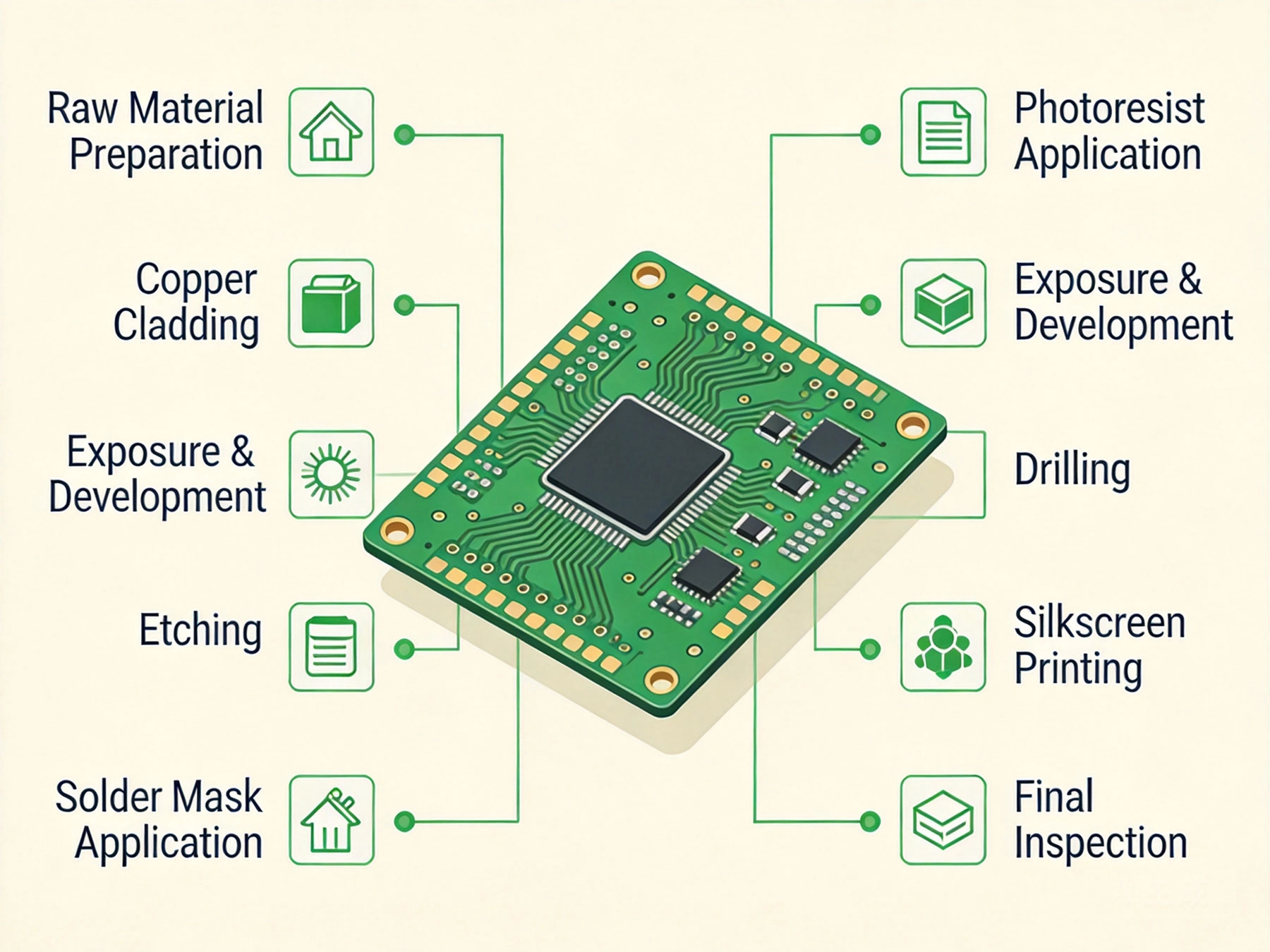
You have spent weeks perfecting your Pcb Design. Your Gerber Files are ready, your components are on order, and you are eager to see your creation come to life. But what happens between hitting "send" on those design files and receiving a stack of green boards at your door?
Understanding the PCB Fabrication process helps you appreciate the craftsmanship involved, communicate more effectively with your manufacturer, and design better boards that are easier to produce. Here is the complete walkthrough.
Before any physical work begins, your manufacturer reviews your Gerber files to ensure they are manufacturable. This is a critical quality checkpoint that prevents expensive mistakes later in the process.
Engineers check your design against the factory capabilities and flag any potential issues:
This step catches problems like traces that are too fine to manufacture, vias that are too small to drill reliably, or spacing violations that would cause shorts. Finding these issues before production begins saves weeks of time and hundreds of dollars.
Your board is cut from a larger panel of substrate material. The panel size depends on your board dimensions and how many boards can be nested efficiently.
Standard FR4 is the most common substrate. It consists of woven glass fabric impregnated with epoxy resin. The "FR" stands for Flame Retardant, and the material is rated by its glass transition temperature (Tg):
The copper-clad panel is cut to size using CNC routers or shears. For Multilayer Boards, inner layer cores are prepared and cleaned before lamination.
Panels go through a thorough cleaning process including scrubbing and chemical treatment. Any contamination at this stage can cause delamination or plating failures later. This step is non-negotiable in quality fabrication.
Drilling is one of the most critical and expensive steps in PCB Fabrication. Every hole, from tiny vias to larger mounting holes, is CNC drilled with precision.
| Hole Type | Typical Diameter | Drill Speed | Notes |
|---|---|---|---|
| Microvia | 0.1-0.2mm | Very high RPM | Laser drilled for best results |
| Standard via | 0.25-0.5mm | 150-300 krpm | Most common hole size |
| Component hole | 0.6-1.0mm | 60-100 krpm | For ICs and connectors |
| Mounting hole | 2.0-6.0mm | 3-20 krpm | For mechanical fasteners |
Modern PCB drills achieve positional accuracy of 25 microns (0.001 inch) or better. The drill bits themselves are made of tungsten carbide or diamond-coated for durability. A typical production run might use hundreds of different drill sizes.
After drilling, a deburring step removes any raised copper or laminate material around hole entries. The panel is then cleaned to remove drilling debris.
A mislocated or mis-sized hole can ruin an otherwise perfect board. The drilling step requires expensive equipment, precise control, and rigorous quality verification. This is why drilling typically accounts for 15-25% of total fabrication cost.
Raw holes drilled through a PCB are not electrically connected. The copper plating step creates conductive paths through the holes, connecting your layers as designed.
Ipc Standards require minimum copper thickness of 25 microns on hole walls for Class 2 boards and 25-30 microns for Class 3. Quality manufacturers verify this with Cross-section Analysis of sample boards from each production lot.
Quality manufacturers detect these issues through automated inspection and Electrical Testing before the board reaches later stages.
For Multilayer Boards, this step transfers your Circuit Pattern onto the inner copper layers. For 2-layer boards, this step applies to the outer layers directly.
Modern imaging systems achieve resolution of 25 microns (1 mil) or better. The alignment accuracy for multilayer boards is typically 25-50 microns, ensuring that inner layers stack up correctly through all layers.
For multilayer boards, this process is repeated for each inner layer, with alignment targets ensuring precise layer-to-layer registration.
This step removes unwanted copper, leaving only your designed circuit traces. There are two main approaches: subtractive (most common) and semi-additive.
Chemical etching undercuts the copper slightly as it removes material. The ratio of etched depth to lateral undercut is the etch factor. Higher etch factor means straighter sidewalls and better trace definition. For fine traces, a high etch factor is critical to avoid trace width loss.
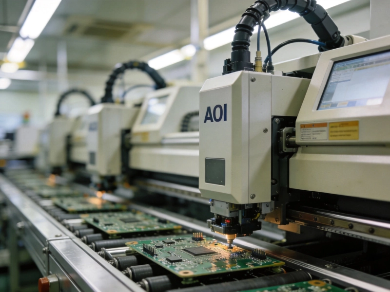
After etching, panels go through automated optical inspection (Aoi) that compares the actual board against the original design data. Aoi detects missing or broken traces, trace width violations, spacing violations, under-etched or over-etched areas, and unwanted copper shorts. Any panels failing inspection are routed for rework or scrapping.
For multilayer boards (4+ layers), this step bonds all layers together into a single unified board. This step is unique to Multilayer Fabrication and does not apply to 2-layer boards.
Misalignment during lamination causes layer-to-layer registration errors. The acceptable tolerance is typically 50-75 microns for standard multilayer boards and tighter for high-density designs. Registration errors can cause opens, shorts, or reduced annular rings.
For multilayer boards, the outer layers are now imaged after lamination. For 2-layer boards, this step was completed before plating. The process is identical to inner layer imaging.
Before outer layer imaging, panels typically receive additional copper plating to achieve the final finished copper weight. This ensures outer layer traces meet thickness specifications after the Etching Process. The outer layer artwork is aligned to the drilled holes using fiducial markers, ensuring that component holes align with your pad patterns on the outer layers.
Soldermask is the green (or other colored) coating that covers the board surface, protecting copper traces from oxidation and preventing solder bridges during assembly. It is what gives most PCBs their characteristic green appearance.
While green is traditional, soldermask comes in many colors including red, blue, black, white, and yellow. Color does not affect performance but can affect visibility of traces and defects during inspection. White mask reflects light best for LED applications. Black provides maximum contrast for Silkscreen readability.
The surface finish protects exposed copper pads from oxidation and provides a solderable surface for component assembly. There are several finish types, each with different characteristics:
| Finish Type | Thickness | Shelf Life | Best For |
|---|---|---|---|
| Hasl / Lead-free Hasl | 1-25 microns | 12 months | Through-hole, general use |
| Enig (Gold/Nickel) | 2-5 uin Au / 120-240 uin Ni | 12 months | SMD, fine pitch, RF |
| Osp (Entek) | 0.1-0.5 microns | 3-6 months | Reflow assembly, economy |
| Immersion Silver | 5-15 microns | 6-12 months | Lead-free, flat surface |
| Hard Gold | 25-100 microns | Indefinite | Edge connectors, wear areas |
For most modern assemblies with fine-pitch components, Enig provides the flattest surface and best Solderability. For through-hole boards with larger components, HASL is cost-effective and reliable. Osp is the most economical but has the shortest shelf life.
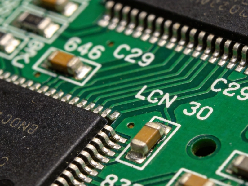
Silkscreen applies the white text, logos, and reference designators that identify components and provide assembly guidance.
Typical silkscreen elements include reference designators (R1, C2, U3, etc.), component outlines, polarity markers, part numbers and revision codes, and warning labels and certifications.
Silkscreen is applied over the soldermask and cannot overlap pads or vias. The minimum line width and text height are limited by the printing process. Fine-pitch components may not have individual reference designators printed due to space constraints.
The final physical shaping of your board: cutting it from the production panel to its final dimensions and separating individual boards from panelized designs.
Ipc Standards allow dimensional tolerances of 0.1mm for board dimensions and 0.05mm for feature location. Quality manufacturers maintain tighter tolerances through proper tooling and measurement verification.
For castellated holes (edge plating for module mounting), additional routing or milling operations create the half-hole pattern along board edges.
Every board should be tested for electrical continuity before shipment. This catches manufacturing defects that could cause assembly failures or field returns.
A single bad board in a batch of 100 means potential field failures and warranty costs that far exceed the cost of testing every board. Quality manufacturers test 100% of production boards, not just samples.
The final quality gate before your boards ship. Visual inspection and packaging complete the fabrication process.
Pcb Fabrication quality is governed by industry standards that define acceptable criteria for various applications:
Ipc Certification specifies everything from minimum conductor width and spacing to hole wall copper thickness and soldermask adhesion. Class 3 boards undergo more rigorous testing and documentation requirements than Class 2. Your application determines which class you need.
The journey from Gerber files to green board involves 14 major process steps, sophisticated equipment, skilled operators, and rigorous Quality Control. Understanding this process helps you appreciate the craftsmanship involved and make better design decisions.
Every board you receive represents hundreds of decisions, precise operations, and quality checks. The best PCB designers understand the manufacturing process well enough to design boards that are not just functionally correct, but optimized for reliable, cost-effective production.
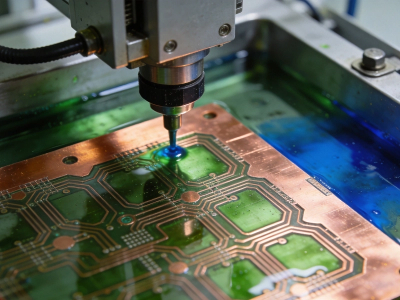
Etching Explained: How Circuit Patterns are Precisely Formed on Copper Clad LaminatesJuly/30/2026
E-Commerce vs. Traditional Sales: How Buying PCB Services Has ChangedJuly/25/2026
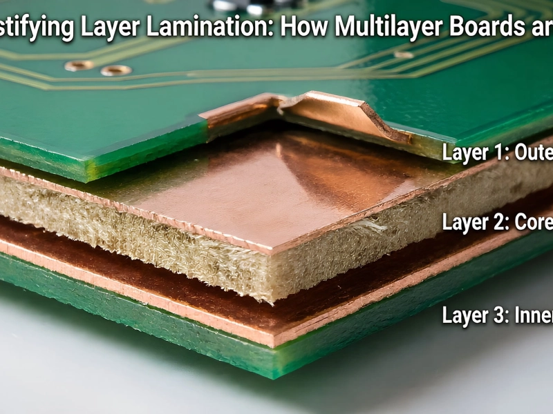
Demystifying Layer Lamination: How Multilayer Boards are BuiltJune/05/2026
Solder Mask and Silkscreen: More Than Just Aesthetics in the PCB ProcessJuly/20/2026
Quality Control 101: AOI, X-Ray, and Electrical Testing in PCB ProductionAugust/10/2026

Surface Preparation: The Critical Steps Before Component AssemblySeptember/16/2026

How Automation is Revolutionizing China's PCB SectorJune/03/2026
Is PCB Fabrication in China Still the Most Cost-Effective Option? A 2026 AnalysisJuly/27/2026