Open Nav
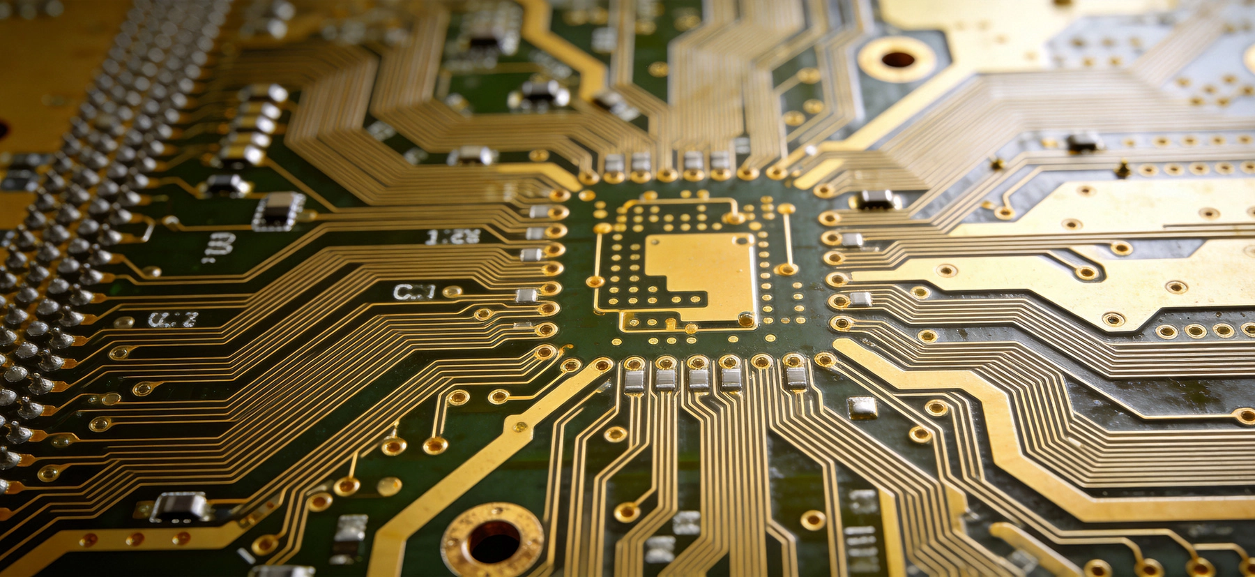
Thirty years ago, a 6 mil trace and 6 mil space was considered "fine line" technology. Today, leading manufacturers routinely produce 3 mil traces with 3 mil spaces, and advanced facilities push boundaries to 2 mil or even smaller. This dramatic reduction in minimum trace and space capabilities hasn't just enabled smaller electronics—it's fundamentally changed what's possible in Pcb Design, making products from smartphones to medical devices smaller, faster, and more powerful than ever before.
But how did we get here, what capabilities exist today, and what does the future hold for trace and space technology? Understanding this evolution matters for anyone designing electronics, sourcing Pcb Manufacturing services, or planning products for tomorrow's markets.
The journey from relatively coarse trace geometry to today's ultra-fine capabilities reflects advances across multiple domains: imaging systems, chemical processing, material science, and quality control. Each step forward built upon previous capabilities, with the electronics industry's relentless drive toward miniaturization providing constant pressure for improvement.
Through the 1990s, 8 mil traces with 8 mil spaces represented standard Pcb Manufacturing capabilities across most facilities. This geometry provided sufficient copper carrying capacity for most applications while maintaining reliable manufacturability with available technology. For reference, 8 mil equals 0.2 millimeters—roughly twice the thickness of a human hair.
The limitations of 8 mil geometry became apparent as electronics demanded higher density. A typical component with 0.8 mm pitch required careful routing planning, and four-layer boards often couldn't accommodate the routing needed for complex designs. As surface mount components decreased in size and functionality increased per unit area, the industry needed finer geometry capabilities.
By the early 2000s, 6 mil traces and spaces had become widely available as standard capabilities at many PCB fabricators. This reduction represented significant progress—25% finer geometry enabled 56% more routing density in the same board area. For many applications, this increase in routing capability enabled designs previously requiring additional layers or larger board footprints.
The transition to 6 mil capabilities relied on improved dry film photoresists, better exposure systems, and enhanced etching chemistry. Laser direct imaging (LDI) systems began replacing traditional contact printing, enabling more precise image transfer and tighter control over trace geometry. These investments paid dividends as consumer electronics demanded smaller form factors without sacrificing functionality.
By the mid-2000s, 4 mil traces and spaces marked the transition from advanced to leading-edge capabilities. This geometry represented another 33% reduction in trace width, enabling 125% increase in routing density compared to 6 mil capabilities. Applications demanding maximum density—smartphones, wearable devices, and high-performance computing—began specifying 4 mil geometry routinely.
Achieving 4 mil capabilities required significant investments: LDI exposure systems became standard, etching processes needed precise control, and inspection systems advanced to detect defects at these smaller dimensions. Quality control became more critical as well—tiny variations in processing that were acceptable at 8 mil could cause yield problems at 4 mil. Manufacturers who mastered these processes gained competitive advantages in high-density applications.
Today's leading PCB fabricators offer 3 mil traces and spaces as standard capabilities for most technologies, with 2 mil available for advanced applications. This geometry enables routing densities more than three times higher than the 8 mil era, supporting the incredible functionality packed into modern electronics. A smartphone's main board, for example, typically uses trace geometries in the 3-4 mil range to accommodate thousands of connections in a compact footprint.
Pushing beyond 2 mil introduces significant challenges. At these dimensions, resist systems, etching chemistry, and material properties become critical factors. Copper plating uniformity, dielectric characteristics, and Signal Integrity considerations all change at micro-scale geometries. Nonetheless, specialized facilities producing IC substrates and advanced packaging operate at 1 mil and below, demonstrating what's technically possible with sufficient investment and expertise.
Reducing minimum trace and space capabilities isn't about one breakthrough—it's about simultaneous advances across multiple process steps. Each step in PCB manufacturing had to evolve to support finer geometries, with improvements in one area enabling progress in others.
Traditional PCB manufacturing used contact printing—photoplots pressed against coated copper to transfer circuit patterns. This approach has inherent limitations: photoplot resolution, contact quality variations, and diffraction effects all limit minimum feature size. For 8 mil geometries, contact printing worked adequately, but finer capabilities required different approaches.
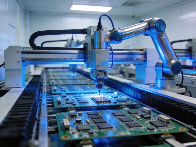
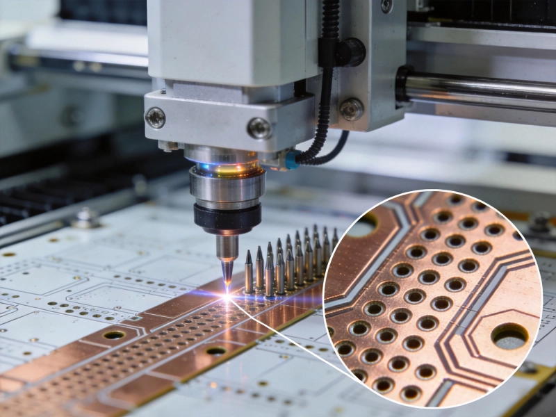
Laser direct imaging (LDI) systems eliminate the photoplot entirely, writing circuit patterns directly onto photoresist-coated boards using computer-controlled lasers. Modern LDI systems achieve spot sizes below 25 microns (approximately 1 mil), enabling precise pattern transfer with minimal distortion. These systems also eliminate photoplot costs and reduce setup time, making fine line capabilities economically viable for production volumes.
The evolution from contact printing to LDI represents perhaps the most significant enabler of fine line capabilities. Without the precision and control that LDI provides, achieving consistent 3 mil and 2 mil geometries would remain impractical for most manufacturers.
Photoresist quality directly affects achievable trace and space dimensions. As geometries decreased, photoresist systems evolved to provide higher resolution, better sidewall formation, and improved etch resistance. Dry film resists—the workhorse of PCB manufacturing for decades—saw formulations optimized for fine line applications, with thinner coatings and enhanced resolution characteristics.
For the most demanding applications, liquid photoresists (often applied by spray coating) replaced dry films. Liquid systems can achieve more uniform, thinner coatings with excellent resolution, though they require more complex processing equipment. Advanced liquid resist systems achieve line resolution capabilities below 2 mil, enabling today's most aggressive geometries.
Resist systems also improved in adhesion characteristics and thermal stability. Fine line traces with smaller cross-sections heat more during operation than larger traces, so resist must withstand processing temperatures without degrading. These improvements in resist technology have been essential enablers of fine line capabilities.
Chemical etching removes unwanted copper from circuits, and as geometries decreased, etching processes needed unprecedented precision. Traditional etching chemistry with aggressive copper removal rates caused undercut—the etchant removing copper sideways as well as vertically. At larger trace widths, undercut could be compensated for in design. At fine geometries, even small undercut amounts significantly affect final trace dimensions.
Modern etching systems use carefully controlled chemistry with temperature, spray pressure, and chemistry composition precisely regulated. Additives in etching solutions reduce undercut while maintaining reasonable etch rates. Some facilities employ pulse etching—alternating etching and rinse cycles—to improve control. These advances enable consistent trace widths within tight tolerances at fine geometries.
Micro-etch cleaning processes before resist application and after etching also improved. Consistent surface preparation is essential for fine line capabilities—any contamination or surface irregularity affects pattern transfer and etching uniformity. Advanced cleaning and surface preparation processes became standard as manufacturers pushed toward smaller geometries.
As trace dimensions decreased, visual inspection became inadequate for quality control. Automated Optical Inspection (AOI) systems evolved to detect defects at 3 mil and 2 mil geometries, with high-resolution cameras and sophisticated image processing algorithms. Modern AOI systems can identify misregistration, shorts, opens, and other defects that would escape human visual inspection at fine geometries.
For verification beyond what's visible optically, electrical testing became essential. Flying probe testers and bed-of-nails fixtures verify electrical continuity and isolation, catching shorts and opens that might be invisible but cause functional failures. Testing at 2 mil geometries requires careful test fixture design, but these capabilities have become standard at fine-line manufacturers.
Statistical process control (SPC) also evolved as fine line capabilities matured. Monitoring key process parameters—etch rates, resist thicknesses, exposure settings—became essential for maintaining consistent yields at tight tolerances. Manufacturers who invested in robust SPC systems typically achieved more consistent fine line capabilities than those relying on end-of-line inspection alone.
Reducing minimum trace and space capabilities isn't just a manufacturing challenge—designers must adapt their approaches as well. Electrical characteristics change at fine geometries, manufacturing constraints become more significant, and design rules evolve accordingly. Successful fine line Pcb Design requires understanding these factors.
As traces decrease in width, their current-carrying capacity decreases proportionally—all else being equal. However, designers have several options for maintaining current capacity at fine geometries: increasing copper thickness (using 2 oz or 3 oz copper instead of standard 1 oz), using wider traces where space allows, and accepting higher temperature rises within component specifications.
For many applications, fine line traces carry relatively low-current signals rather than power distribution. Digital buses, control signals, and data paths operate at currents well within fine line capabilities, while power routing uses wider traces or internal planes. Designers must carefully analyze current requirements and allocate appropriate trace widths accordingly.
IPC standards provide guidance on current carrying capacity based on trace dimensions, copper thickness, and acceptable temperature rise. Following these guidelines helps ensure reliable operation, though designers often conduct more detailed analysis using simulation tools for critical applications.
Controlled Impedance requirements become more challenging at fine geometries. Impedance depends on trace width, dielectric thickness, dielectric constant, and reference plane configuration. As traces become narrower, achieving specific impedance values requires tighter control over all contributing factors. Small variations in trace width or dielectric thickness have larger effects at fine geometries.
For Controlled Impedance applications at fine geometries, designers often specify tighter tolerances for trace width and dielectric thickness. Manufacturers respond with enhanced process controls—measuring and compensating for process variations through post-processing etch compensation and other techniques. These capabilities add cost but are essential for high-speed digital designs at fine line geometries.
Designers must work within manufacturer capabilities when specifying fine line geometries. Not all features can be simultaneously minimized—for example, minimum annular ring, drill size, and via geometry all interrelate with trace and space capabilities. Specifying 3 mil traces alongside large via diameters or wide clearance requirements can create manufacturing challenges.
Leading manufacturers provide design rules specific to their capabilities. These rules specify minimum and preferred dimensions for various features, balancing manufacturability with design requirements. Working within these rules—rather than pushing every parameter to its minimum—typically yields better yields and more reliable products.
At high frequencies, trace geometry affects Signal Integrity in ways beyond simple current carrying capacity. Skin effect causes current to concentrate near trace surfaces, and as traces become narrower, resistance increases. For very high-frequency signals, these effects matter and designers must account for them in analysis and design.
Dielectric losses also become more significant at fine geometries and high frequencies. Signals spending more time near the dielectric material experience greater attenuation. Designers of high-speed interfaces at fine line geometries often specify materials with lower loss tangents and use simulation tools to predict signal behavior under realistic conditions.
Not all PCB manufacturers offer the same fine line capabilities, and claimed capabilities don't always translate into consistent production results. Selecting the right manufacturer for fine line PCBs requires careful evaluation of capabilities, processes, and quality systems.
Specification sheets list capabilities, but they don't guarantee consistent results. Look for manufacturers who can demonstrate their fine line capabilities through samples, customer references, and documentation. Ask about actual production experience at the geometries you require—not just capability statements.
Ask about yield rates at fine geometries. Manufacturers genuinely capable of consistent fine line production track their yields by feature size and can provide realistic expectations. If a vendor can't discuss yield data, it may indicate they lack experience or control over fine line processes.
Ask about the specific equipment used for fine line capabilities. Laser direct imaging systems are virtually essential for 3 mil and below—manufacturers using contact printing for these geometries likely struggle with consistency. Similarly, ask about etching systems—do they have controlled chemistry with precise parameter regulation?
Inspection capabilities matter as well. AOI systems rated for fine line geometries, flying probe testers, and appropriate fixture capabilities all indicate serious commitment to fine line production. Manufacturers who invest in these capabilities typically deliver more consistent results.
ISO 9001 certification provides baseline quality system assurance, but for fine line capabilities, look for evidence of statistical process control. Manufacturers who monitor key parameters, conduct regular capability studies, and use data to drive process improvement typically achieve better consistency at tight tolerances.
Ask about process validation procedures—how does the manufacturer qualify new designs at fine line geometries? Comprehensive pre-production evaluation, first-article inspection, and verification procedures reduce risk when moving to production. Manufacturers with robust validation processes typically provide more reliable results.
PCB trace and space capabilities haven't plateaued—they continue advancing, driven by the relentless demand for higher density and functionality. Emerging capabilities promise further reductions, though each step forward requires overcoming significant technical and economic challenges.
Specialized manufacturers currently produce at 1.5 mil and below for specific applications, particularly IC substrates and advanced packaging. These capabilities represent the cutting edge of what's technically possible today, though costs remain high and applications relatively specialized. As these technologies mature and costs decrease, sub-2 mil capabilities will likely become more widely available.
Pushing below 1 mil introduces fundamental material and process challenges. At these dimensions, conventional photoresists struggle with resolution, etching chemistry must achieve near-perfect sidewall profiles, and inspection capabilities approach optical limits. Nonetheless, research continues, and breakthrough material or process developments could accelerate progress.
Traditional PCB manufacturing is subtractive—copper is plated, then unwanted copper is etched away. Additive approaches—building up traces only where needed—eliminate etching and its limitations. Various additive and semi-additive processes show promise for ultra-fine geometries, potentially enabling trace and space capabilities beyond what's practical with subtractive methods.
Additive approaches also reduce material waste and can simplify some manufacturing steps. While currently specialized and relatively expensive, additive processes may become more mainstream as the industry seeks solutions to the limitations of subtractive approaches at very fine geometries.
Future capabilities may combine multiple technologies rather than relying on single breakthroughs. For example, hybrid approaches might use conventional subtractive processes for general routing with additive methods for critical fine features. Similarly, laser direct imaging might combine with advanced etching to achieve capabilities beyond what either technology provides alone.
These hybrid approaches acknowledge that fine line requirements vary across designs—not every trace needs to be at minimum dimensions. By using appropriate technologies for different features, manufacturers can balance capabilities with costs and yields.
Understanding trace and space capabilities helps, but applying that knowledge effectively requires practical guidance. Here are key considerations for leveraging fine line capabilities in your designs.
Don't specify finer geometries than your design actually needs. If 4 mil traces accommodate your routing requirements, specify 4 mil rather than pushing to 3 mil unnecessarily. Finer geometries increase costs and reduce yields without providing meaningful benefits if your design doesn't require them. Work with your manufacturer to identify optimal geometries for your specific requirements.
Fine line PCBs require careful verification before and after production. Electrical testing becomes more critical as defect sizes decrease. Plan adequate testing resources and budget for comprehensive verification. For complex designs, consider working with manufacturers who provide design for manufacturing (DFM) reviews to identify potential issues before production.
Specify tolerances that match your manufacturer's capabilities. Asking for tolerances tighter than what a manufacturer can consistently achieve leads to frustration and reduced yields. Instead, work within realistic tolerances and design your product to accommodate those tolerances. Manufacturers appreciate realistic specifications and typically deliver better results when requirements align with their capabilities.
Fine line capabilities often come with higher per-board prices, but consider total cost including yields, testing, and potential redesigns. A manufacturer with slightly higher prices but better yields and consistency may actually cost less overall than the cheapest vendor. Evaluate total cost rather than simply comparing unit prices.
The evolution from 8 mil to 2 mil trace and space capabilities represents remarkable progress, enabling electronics that would have been impossible three decades ago. Today's smartphones, wearable devices, and compact medical devices all depend on fine line capabilities to pack remarkable functionality into small form factors.
Understanding these capabilities—what's possible, what's practical, and how to work with manufacturers who can deliver them—helps designers create better products. By matching design requirements to Manufacturing Capabilities, specifying realistic tolerances, and planning appropriate verification, designers can leverage fine line capabilities effectively.
As capabilities continue advancing, the possibilities will expand further. Sub-2 mil geometries, additive manufacturing approaches, and hybrid technologies promise even greater density and functionality. The journey toward finer trace and space capabilities continues, driven by the relentless innovation of the electronics industry and the relentless demand for smaller, more powerful products.

Top Trends Shaping the Chinese PCB Manufacturing Industry in 2026May/21/2026
Why Global Brands Are Turning to PCB Fabrication in China in 2026May/21/2026
Decoding the Spec Sheet: Understanding a Factory's PCB Fabrication CapabilitiesJune/11/2026
24-Hour Turnaround: Is it Possible and How Does it Work?May/21/2026
The Benefits of Combining PCB Fabrication and AssemblyMay/22/2026
How to Find the Right PCB Fabrication Partner in ChinaJune/02/2026
Demystifying Layer Lamination: How Multilayer Boards are BuiltJune/05/2026
The Art of Drilling: Mechanical vs. Laser Drilling in Modern PCB ManufacturingJune/26/2026