Open Nav

With continuous technological upgrades and massive production capacity, PCB Fabrication in China remains the strategic choice for global electronic supply chains.
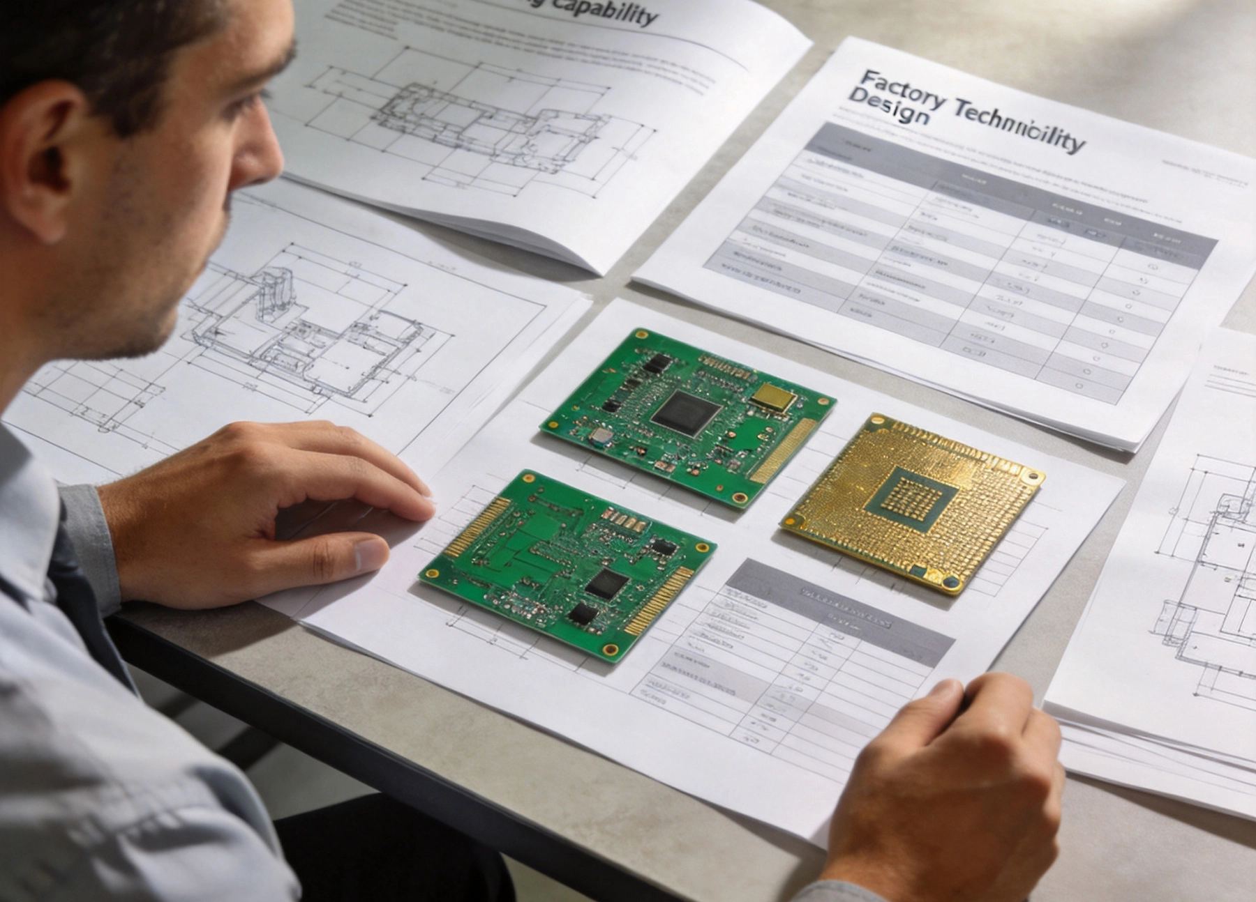
Why Capability Statements Matter: Matching Your Design Needs to Factory StrengthsOctober/09/2026You have a design. You need it built. You search for manufacturers, compare websites, and send out requests for quotes. Days or weeks later, you get responses back—some promising, some disappointing, some mysteriously silent. Somewhere in this process, you might be making a fundamental mistake: tr...
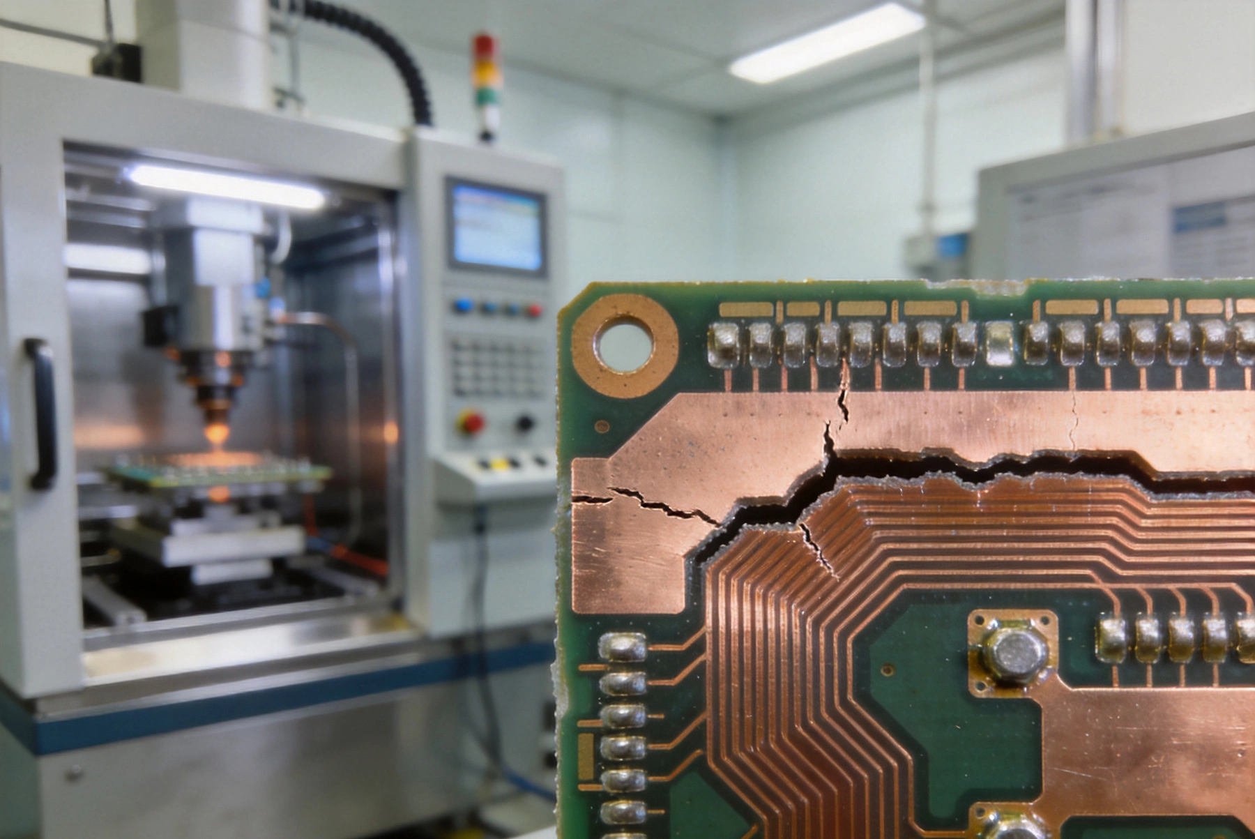
Reliability Testing for Complex HDI Boards: Ensuring Long-Term PerformanceSeptember/30/2026Complex HDI boards push the limits of PCB manufacturing. With microblind vias, dense routing, thin dielectrics, and a proliferation of BGA packages at 0.4 mm pitch and finer, these boards carry more electrical and mechanical risk per square centimeter than almost any other class of electronic asse...
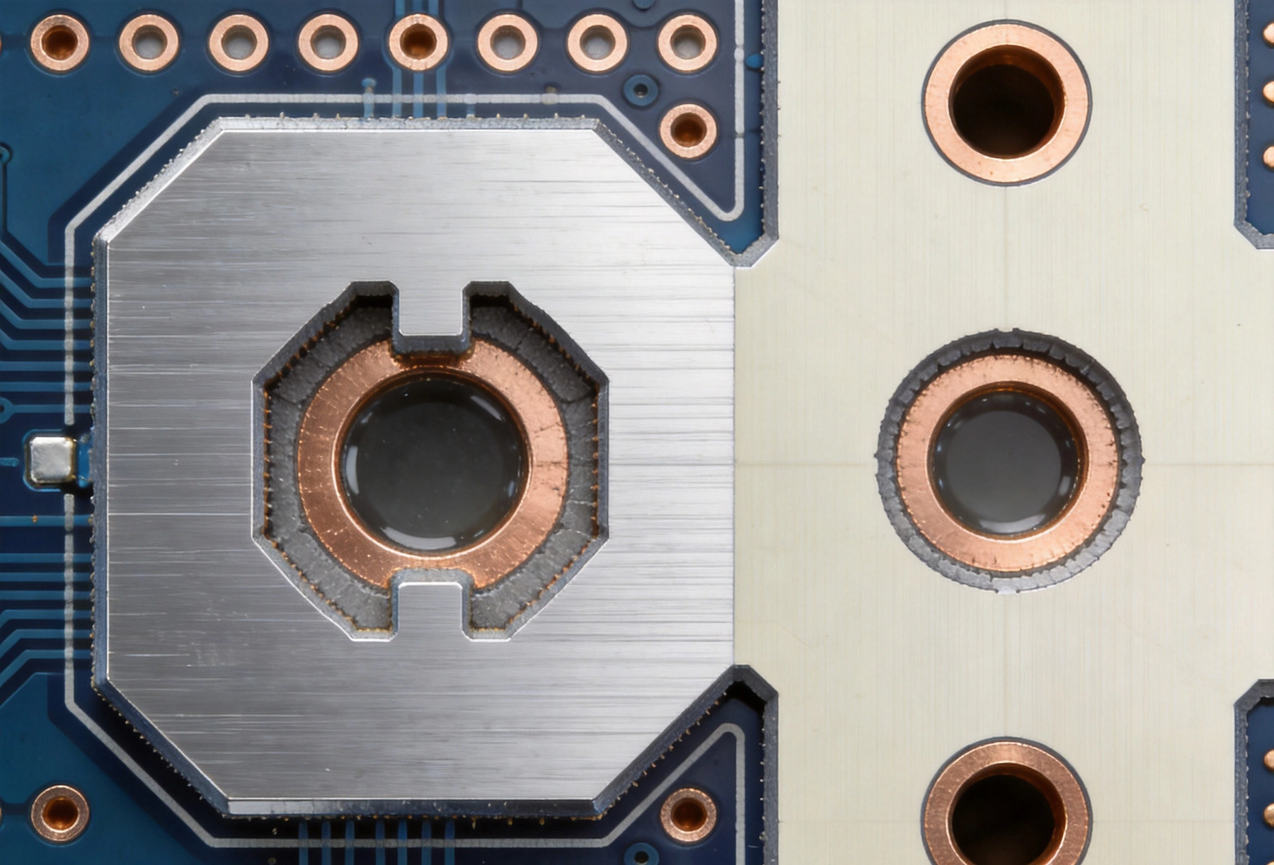
Back-drilling and Via-in-Pad: Advanced Capabilities for High-Speed DesignsSeptember/29/2026High-speed digital designs operating at multi-gigabit data rates demand signal integrity performance that conventional PCB via structures simply cannot deliver. Signal frequencies in modern interfaces such as PCIe 5.0/6.0, 400G Ethernet, DDR5, and USB4 push well into the tens of GHz, where even mi...
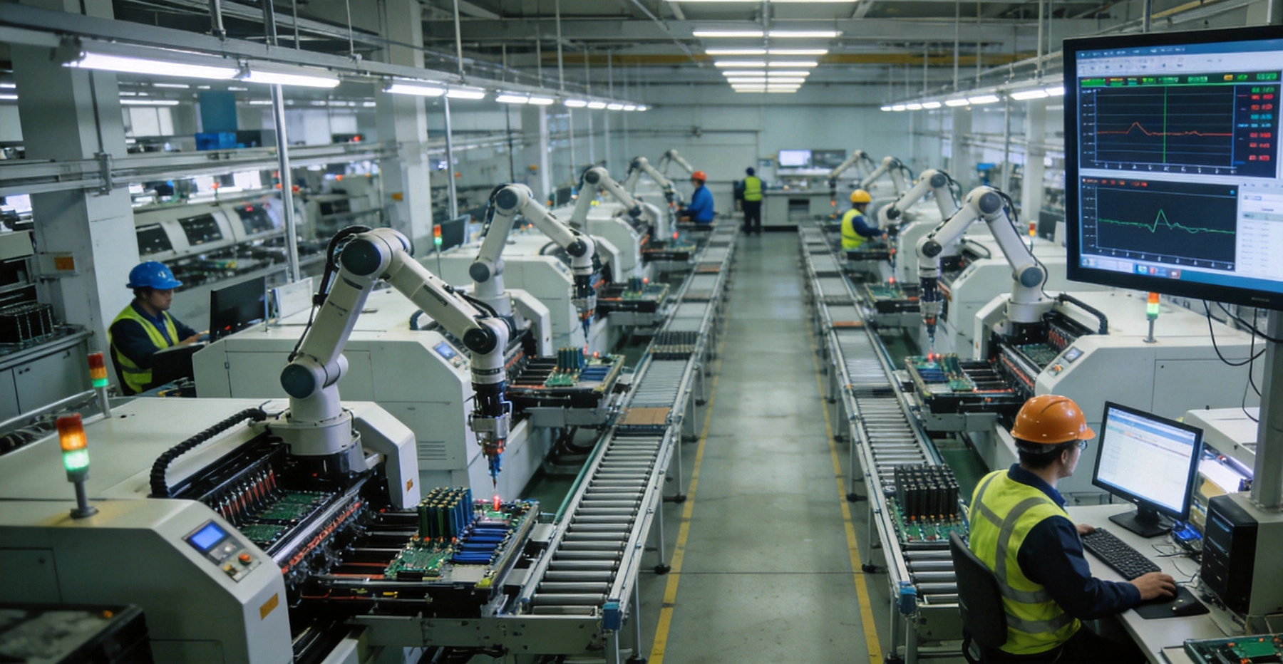
Choosing the Right Assembly Partner: Capabilities, Capabilities, Certifications, and CapacitySeptember/28/2026The contract electronics manufacturing market is large, fragmented, and varies enormously in capability. On one end are small shops with a single pick-and-place line and limited inspection equipment. On the other are large-scale facilities with fully automated assembly lines, X-ray and AOI inspect...
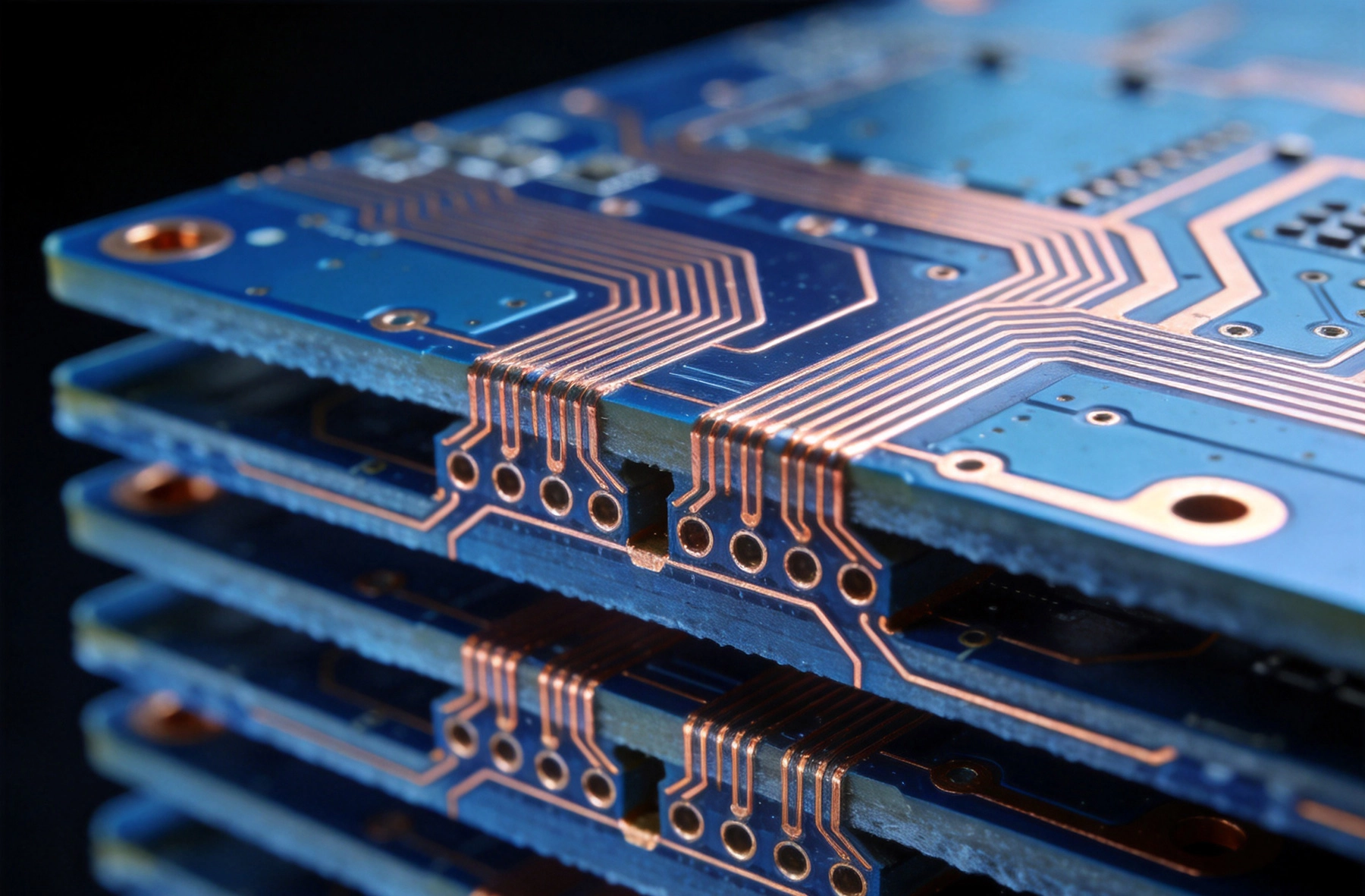
Cost Drivers in HDI and Multilayer PCB Fabrication: What Engineers Need to KnowSeptember/26/2026The cost of an HDI or multilayer PCB is not a simple function of board size or layer count. It is the result of many interacting factors — some driven by your design choices, others by the capabilities and processes of the fabricator. Understanding these cost drivers is essential for engineers who...
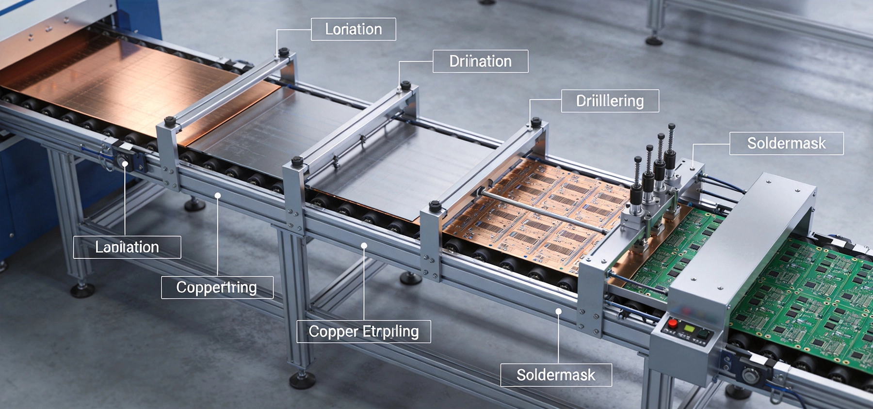
Visualizing the Flow: An Infographic Guide to How Your PCB is MadeSeptember/24/2026You upload your Gerber files, wait a few days, and a finished PCB arrives at your door. But what actually happens in between? Understanding the manufacturing process—really understanding it, step by step—makes you a better designer. When you know how copper is etched, why lamination pressure matte...
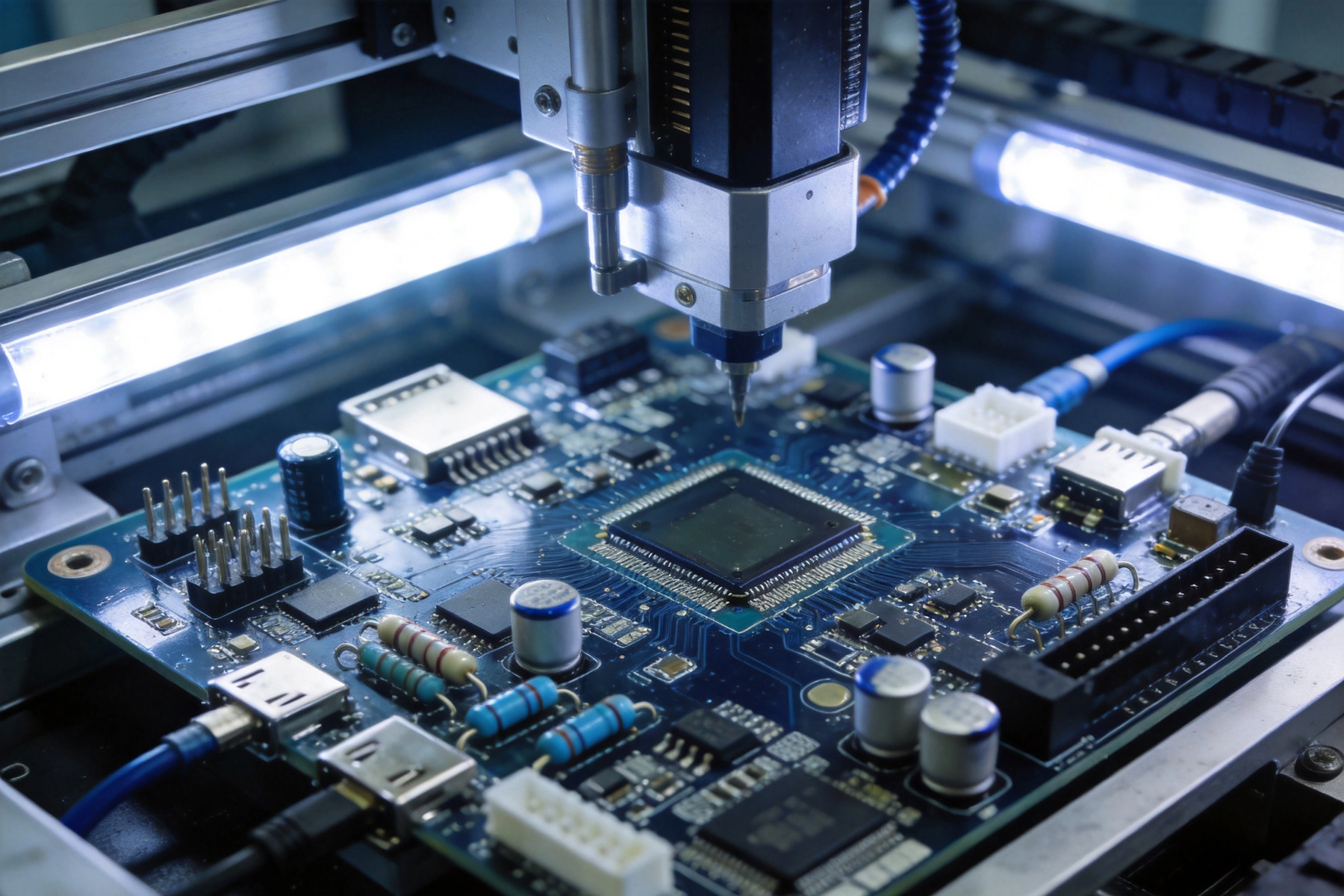
Tailored Solutions: Why Off-the-Shelf PCBs No Longer Cut It for Modern TechSeptember/23/2026The era when standard PCB designs could satisfy most product requirements has passed. As technology advances across industries from artificial intelligence to electric vehicles, the demands placed on electronic hardware have grown far beyond what generic solutions can address. Product engineers an...

Intellectual Property Protection: Safeguarding Your Designs When Using External ServicesSeptember/21/2026When you outsource PCB manufacturing or assembly to external services, you entrust your most valuable technical assets to third parties. Your circuit designs, firmware, proprietary algorithms, and manufacturing know-how represent years of development and substantial investment. Without proper safe...
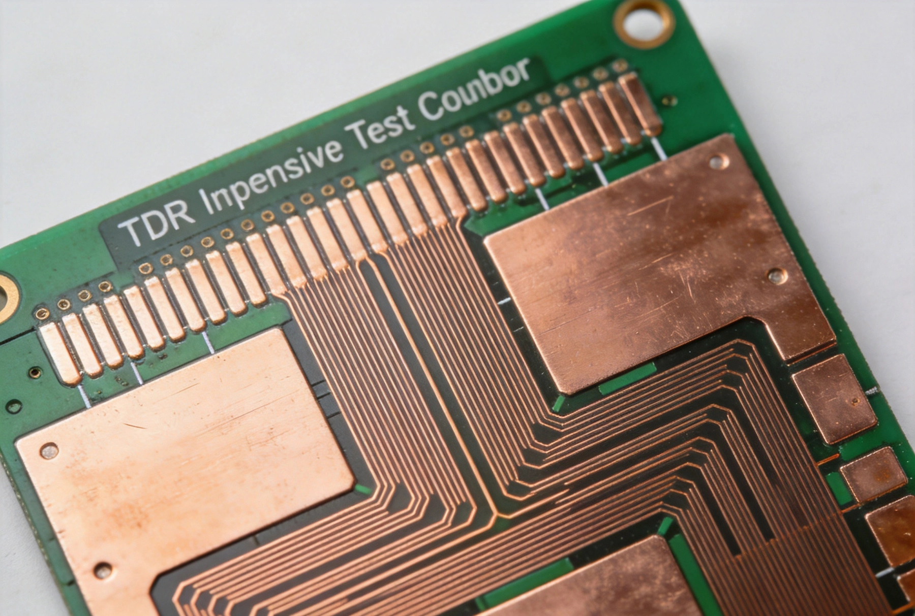
Controlled Impedance: Measuring a Manufacturer's Ability to Hit Tight TolerancesSeptember/20/2026In high-speed digital and RF design, controlled impedance is not a nice-to-have—it is a hard requirement. A 100 Ω differential pair that drifts to 112 Ω reflects enough signal energy to close the eye diagram on a 10 Gbps link. A 50 Ω RF trace that shifts to 54 Ω creates a 4 % VSWR mismatch that de...
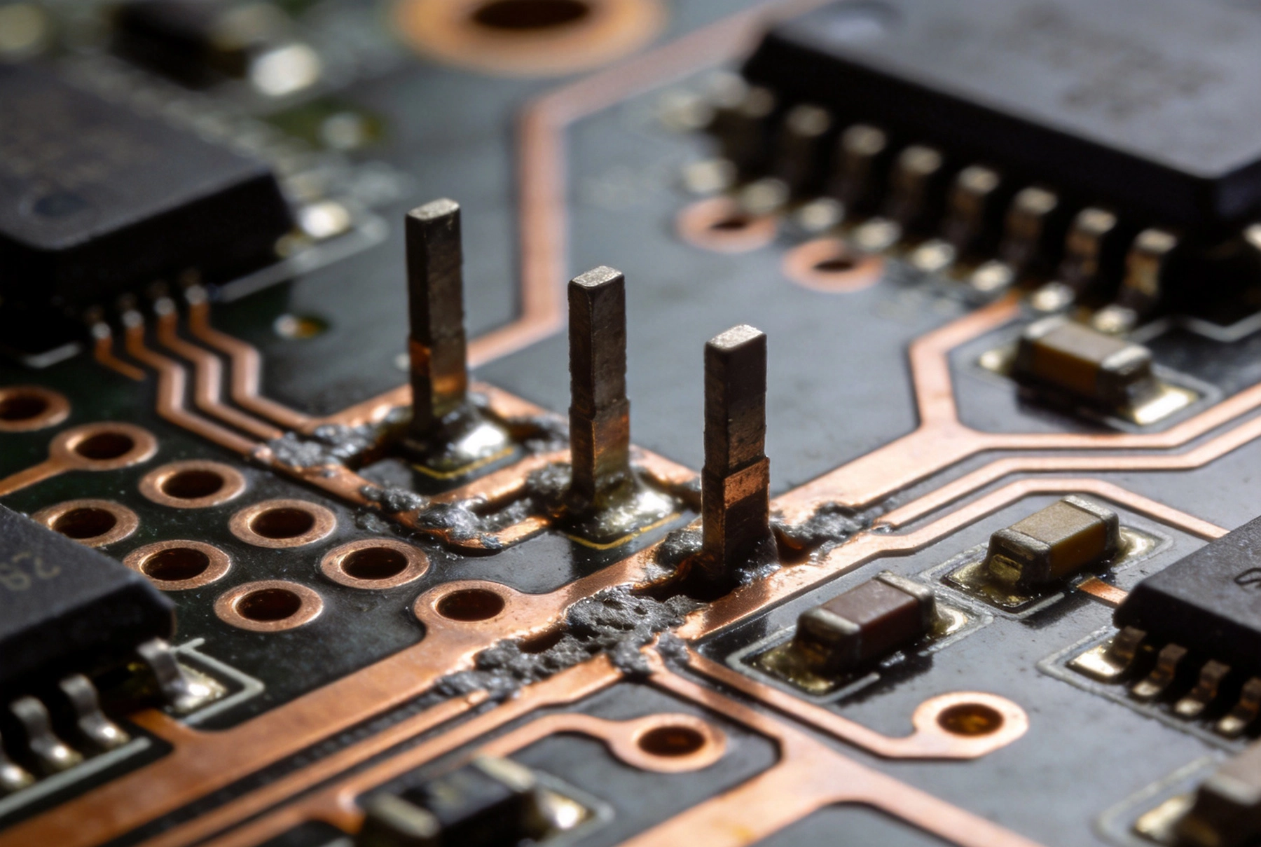
Common Defects in PCB Assembly and How Manufacturers Prevent ThemSeptember/18/2026No manufacturing process is perfect, and PCB assembly is no exception. Even in state-of-the-art facilities with automated lines and AI-powered inspection, defects occur — though at far lower rates than in facilities relying on older equipment or manual processes. The key difference between a high-...
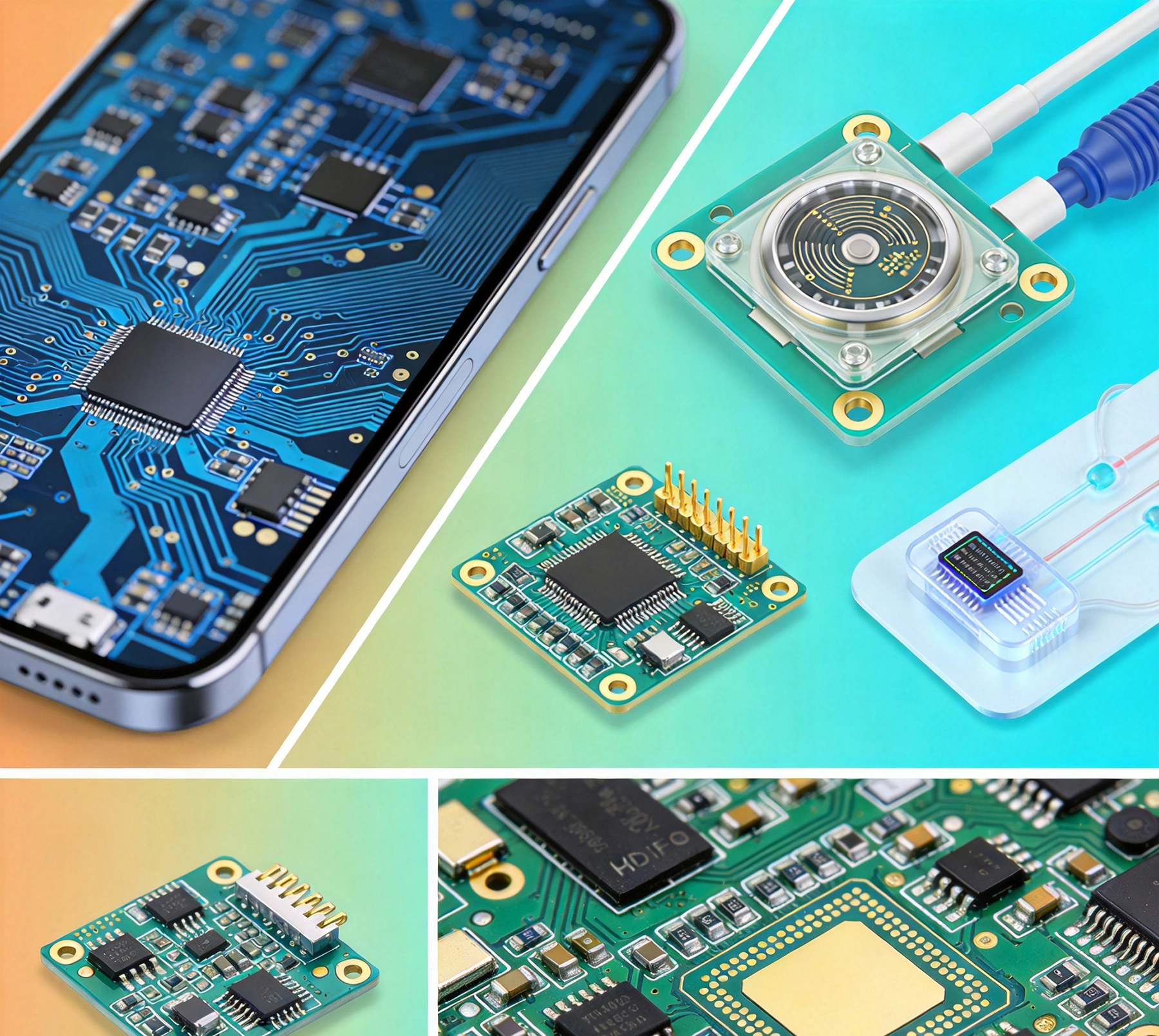
Applications Driving the Demand for HDI PCBs: From Smartphones to Medical DevicesSeptember/17/2026High-Density Interconnect (HDI) PCB technology was born from a single imperative: make electronic devices smaller without sacrificing functionality. What began as a specialized fabrication technique for mobile phones has evolved into a foundatonal technology across dozens of industries. Today, HDI...
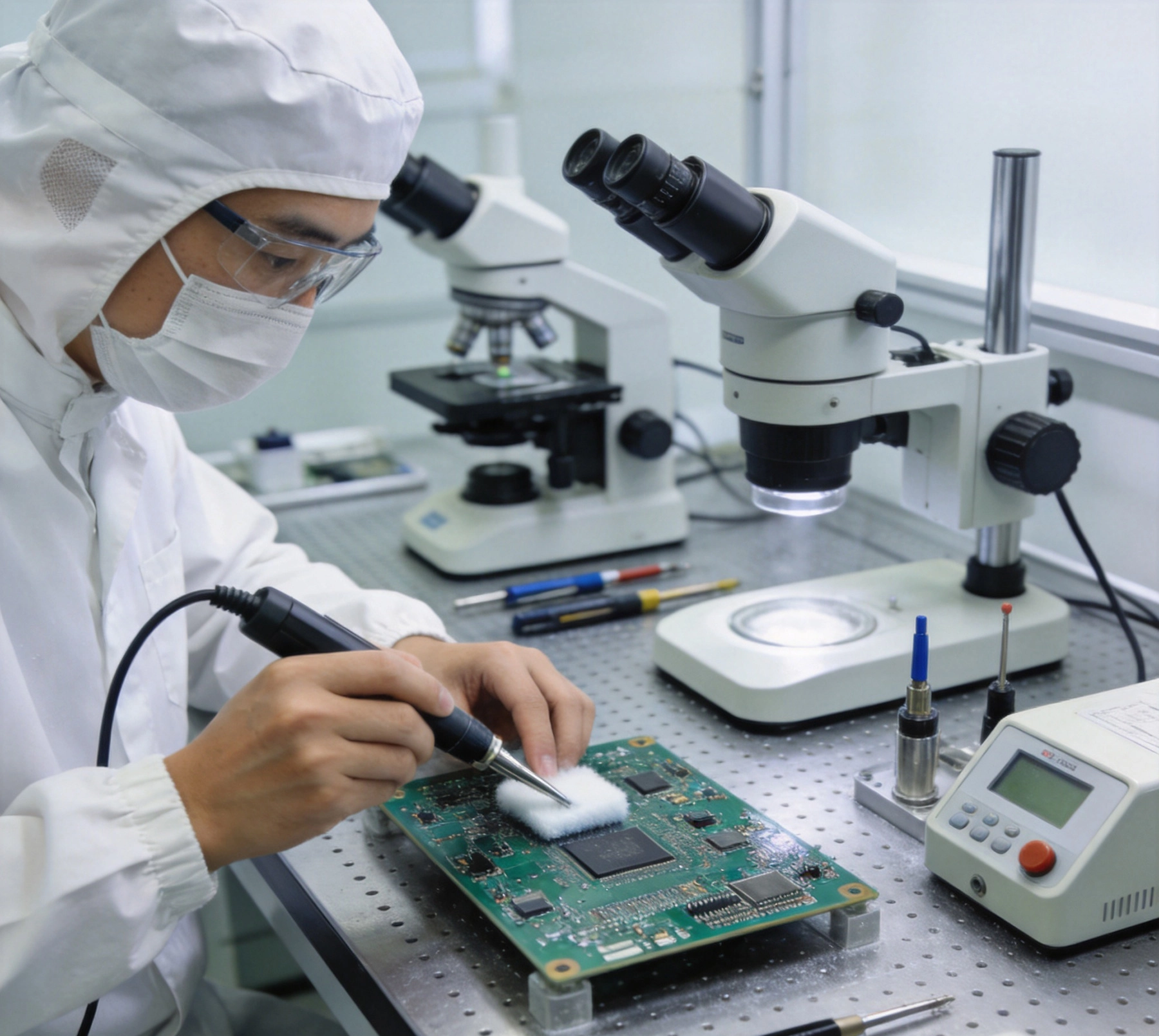
Surface Preparation: The Critical Steps Before Component AssemblySeptember/16/2026Every reliable solder joint begins long before the paste is dispensed or the reflow oven reaches temperature. The quality of the bare printed circuit board surface arriving from fabrication—and the preparation it receives before assembly—determines whether components will form strong, reliable con...