Open Nav

Every reliable solder joint begins long before the paste is dispensed or the reflow oven reaches temperature. The quality of the bare printed circuit board surface arriving from fabrication—and the preparation it receives before assembly—determines whether components will form strong, reliable connections or fail prematurely in the field. Surface preparation is not an optional step or a finishing touch; it is the foundation upon which assembly quality rests.
This article examines the critical surface preparation steps that occur between PCB Fabrication and component placement, explaining why each step matters, what can go wrong when preparation is neglected, and how professional assembly services ensure the board surface is ready for the demanding Smt Assembly process.
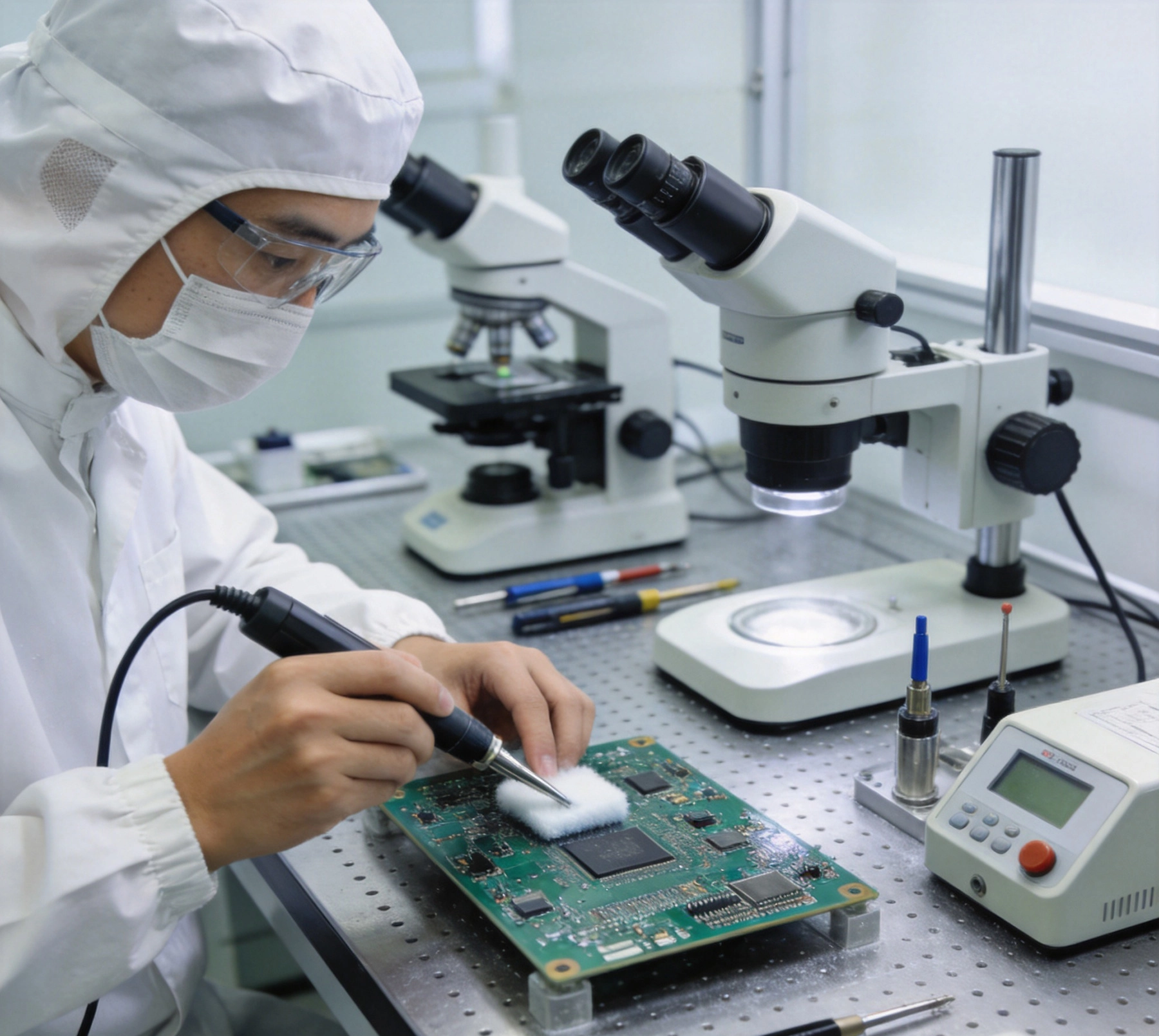
The copper traces and pads of a PCB are exposed to multiple processing steps during fabrication including etching, plating, Solder Mask application, and surface finish coating. Each step leaves residues that can interfere with solder wetting—the fundamental process by which molten solder flows and bonds to the metal surface. Contaminants ranging from fingerprints to chemical residues create weak points in the solder joint that may pass initial testing only to fail months or years later.
Modern Surface Mount Technology places exacting demands on surface quality. Fine-pitch components with ball grid arrays and quad flat no-lead packages require near-perfect surface conditions to achieve reliable connections across hundreds or thousands of individual pads. Even minor contamination causes bridges, voids, or incomplete joints that require rework or result in field failures.
The stakes extend beyond immediate assembly yields. Poor solder joint reliability contributes to customer returns, warranty claims, and reputational damage that far exceeds the cost of proper surface preparation. In industries like automotive, medical devices, and aerospace where failure carries serious consequences, surface preparation quality is treated as a non-negotiable requirement.
Professional assembly services begin with a thorough inspection of incoming PCBs. This incoming Quality Control step identifies surface conditions that might cause assembly problems and documents any issues to be addressed before production begins.
Trained inspectors examine boards under magnification for visible contamination, scratches, fingerprints, or discoloration that indicates oxidation or chemical attack. Solder Mask coverage is checked for completeness, particularly around pad areas where mask pullback could expose copper to contamination. Edge connector areas receive special attention since handling during fabrication and shipping commonly introduces surface defects in these regions.
For boards requiring stringent reliability, cleanliness testing provides quantitative data beyond what visual inspection reveals. Ion chromatography identifies Ionic Contamination from Flux Residues or chemical processing that could cause electrochemical migration under bias. The test involves extracting contaminants from the board surface and analyzing the extract for chloride, sulfate, and other ions that indicate inadequate rinsing or contamination from the fabrication process.
Other cleanliness assessment methods include Surface Insulation Resistance (SIR) testing, which measures resistance between adjacent traces under humid conditions, and visual inspection under ultraviolet light to reveal organic contamination that may not be visible under white light.
Copper surfaces naturally oxidize when exposed to air, forming copper oxide layers that interfere with solder wetting. The thickness and character of this oxide layer determines whether the surface can be successfully soldered without aggressive flux or special treatment. Visual indicators—dull or Rainbow-colored surfaces—suggest excessive oxidation that may require treatment before assembly.
When inspection reveals contamination or oxidation, cleaning processes restore the surface to an assembly-ready condition. The appropriate cleaning method depends on the type of contamination present and the surface finish applied during fabrication.
Organic solvents remove greases, oils, fingerprints, and light contamination from board surfaces. Common solvents used in electronics assembly include isopropyl alcohol (IPA), acetone, and specialized flux removers. Solvent cleaning works through chemical dissolution of contaminants and mechanical action from wiping or agitation.
IPA remains the most widely used solvent due to its effectiveness, availability, and relatively safe handling profile. Pure IPA (99% or higher) without added water or contaminants provides the best results. Lower-grade IPA may introduce additional contamination rather than removing it.
Professional assembly facilities use dedicated cleaning equipment including ultrasonic cleaners for thorough agitation and vapor degreasers for repeatable, controlled cleaning of multiple boards. Manual wiping with lint-free wipers can address local contamination but provides inconsistent results across a full board.
Water-based cleaning systems offer advantages for high-volume assembly operations including environmental compliance and worker safety compared to solvent-based approaches. Aqueous cleaning uses detergents, saponifiers, or mildly alkaline solutions to emulsify and remove contamination.
Deionized (DI) water is essential for aqueous cleaning since tap water introduces Ionic Contamination that defeats the purpose of cleaning. The cleaning process typically involves spray washing, immersion with agitation, and thorough rinsing followed by forced-air drying. Inline aqueous cleaning systems integrated with the assembly line provide consistent processing with documented parameters.
Plasma cleaning represents the most advanced surface preparation technology for electronics assembly. Oxygen or forming gas plasma reacts with organic contamination at the molecular level, converting it to water vapor and carbon dioxide that evacuate the processing chamber. The process also activates the surface by increasing surface energy, improving wettability for subsequent soldering.
Plasma treatment proves particularly valuable for difficult-to-clean surfaces such as recessed features, Blind Vias, and boards with complex geometries where physical cleaning methods cannot reach. The process is repeatable and leaves no residues since contaminants are converted to gases rather than dissolved into liquids.
Equipment for plasma cleaning ranges from benchtop units suitable for Prototype quantities to inline systems processing thousands of boards per day. The cost per board is relatively low once equipment is in place, making plasma treatment economically practical for production volumes.
For stubborn contamination or light oxidation that resists chemical cleaning, microblasting with fine aluminum oxide or other abrasives provides mechanical surface preparation. This method removes a microscopic layer of surface material along with contamination, revealing fresh copper underneath.
Microblasting requires careful control to avoid damaging solder mask edges or removing surface finish. It is typically used as a targeted treatment for specific areas rather than full-board processing. The technique proves useful for restoring pads that have degraded during extended storage or rework operations.
The surface finish applied during PCB Fabrication significantly affects assembly quality and the preparation steps required. Different surface finishes present distinct characteristics that influence cleaning requirements and Solderability.
Hasl-coasted boards feature a layer of solder applied by dipping the board in molten solder with excess solder removed by hot air knives. The resulting surface is relatively rough with inconsistent height across the board due to the natural variation in solder deposition. Hasl provides good Solderability but the uneven surface can cause issues with fine-pitch components where coplanarity matters.
Modern lead-free HASL (using tin-copper or tin-nickel alloys) requires higher processing temperatures than traditional tin-lead HASL, which can affect board warpage and sensitive components. HASL surfaces may require cleaning to remove oxide that develops during storage before assembly.
Enig provides a flat, uniform surface ideal for fine-pitch components and high-reliability applications. The nickel layer provides a reliable barrier against copper diffusion while the thin gold layer protects the nickel from oxidation and dissolves during soldering to expose clean nickel for the solder joint.
Enig surfaces are generally clean upon receipt from fabrication and do not require aggressive cleaning. Light plasma treatment can improve wettability for challenging components or lead-free solders. However, ENIG is susceptible to black pad syndrome—a metallurgical failure mode where the nickel-phosphorus layer becomes oxidized and prevents solder wetting. This defect typically originates in fabrication rather than assembly preparation.
Osp coatings protect bare copper with a thin organic layer that prevents oxidation during storage. The coating is designed to vaporize during the reflow process, exposing fresh copper for soldering. Osp provides excellent flatness for fine-pitch placement and avoids the cost and complexity of precious metal plating.
OSP surfaces require careful handling since the organic coating can be damaged by fingerprints, excessive moisture, or contamination. Light cleaning with IPA may be appropriate for OSP boards, but aggressive cleaning can strip the protective coating. OSP also has limited thermal resistance—multiple reflow cycles may deplete the coating and require reapplication.
Immersion Silver provides a flat, solderable surface with good shelf life when stored properly. The coating is thin (typically 0.1 to 0.4 microns) and can be damaged by excessive handling or abrasion. Immersion tin offers good solderability with the advantage of being less expensive than silver but may develop tin whiskers under certain conditions.
Both immersion finishes benefit from careful handling and minimal cleaning to preserve the coating. Excessive cleaning can remove the protective layer and expose underlying copper to oxidation. If cleaning is necessary, gentle processes using mild solvents are preferred over aggressive aqueous cleaning.
Even the best surface preparation can be undermined by improper storage between cleaning and assembly. Managing shelf life and storage conditions protects the investment in surface preparation and ensures boards arrive at assembly ready for processing.
Temperature and humidity affect surface oxidation rates and the stability of certain surface finishes. Standard storage conditions for most PCB types are 20°C to 25°C with relative humidity below 60%. For moisture-sensitive finishes like OSP, sealed packaging with desiccant maintains surface quality over extended storage periods.
Each surface finish has a defined shelf life after which solderability degrades beyond acceptable levels. OSP coatings typically remain viable for three to six months under normal storage. ENIG maintains solderability for twelve months or more. HASL surfaces can remain solderable for extended periods but may develop oxide requiring cleaning before assembly.
Tracking the date of receipt and storage conditions helps assembly facilities manage inventory rotation and identify boards that may require special preparation before assembly. First-in-first-out inventory practices prevent using degraded boards while acceptable stock remains on shelves.
Fingerprints transfer skin oils that contain salts and fatty acids detrimental to solderability. Bare boards should always be handled by the edges using clean gloves or finger cots. Stackers and magazine rails provide mechanical handling methods that eliminate direct contact with pad areas. These precautions are particularly critical for finishes like OSP that are sensitive to organic contamination.
Professional assembly services follow a defined preparation sequence that addresses common surface conditions and ensures consistent results across all boards processed.
Before any cleaning or treatment, boards are visually inspected to identify obvious defects, damage, or contamination that might require special handling. This inspection also verifies that the correct board revision and surface finish are received as specified in the build documentation.
Even clean-appearing surfaces benefit from activation treatment that removes residual organic contamination and increases surface energy for improved wetting. Plasma treatment or light chemical cleaning prepares the surface for solder paste reflow by creating consistent conditions regardless of minor variations in incoming surface condition.
For critical applications, solderability testing using wetting balance analysis or coupon testing provides quantitative confirmation that the surface will form reliable solder joints. This testing is particularly valuable for boards at the end of their shelf life or when storage conditions are uncertain.
Moisture absorbed by the board laminate or components must be removed before reflow processing to prevent delamination and pop-corning. Boards with absorbed moisture are baked at 125°C to 150°C for four to eight hours depending on thickness. This baking step, while not strictly surface preparation, often precedes assembly and affects surface conditions at the time of processing.
Understanding common errors helps avoid practices that damage surfaces or create problems rather than solving them.
Surface preparation quality is governed by industry standards that define acceptable conditions and test methods.
Professional assembly services maintain procedures compliant with these standards and document process parameters for traceability and continuous improvement.
Not necessarily. Many boards arrive from fabrication in acceptable condition and go directly to assembly without additional cleaning. However, boards stored for extended periods, handled without gloves, or received with visible contamination benefit from surface preparation. Professional assembly services assess each lot and apply cleaning as needed rather than assuming either all-clean or all-need-clean scenarios.
Surface preparation can improve marginally acceptable pads but cannot salvage severely degraded surfaces. Pads with heavy oxidation, black pad defects in ENIG, or contamination bonded to the surface may require re-plating or replacement. Identifying these conditions during incoming inspection prevents wasted assembly effort on boards that cannot produce reliable joints.
Lead-free solders require excellent surface conditions due to their higher liquidus temperatures and reduced wetting ability compared to tin-lead solders. Plasma cleaning provides the most consistent preparation for lead-free applications since it removes organic contamination and activates the surface without risking damage to the underlying finish. For heavily contaminated boards, sequential solvent and plasma cleaning may be appropriate.
OSP typically has a shorter shelf life than ENIG—three to six months compared to twelve months or more. OSP coatings are thinner and more susceptible to damage from handling and environmental exposure. For applications requiring extended storage before assembly, ENIG or HASL surfaces provide more margin for Inventory Management without preparation concerns.
Plasma cleaning is safe for ENIG, OSP, Immersion Silver, and HASL surfaces when process parameters are appropriately set. Oxygen plasma is generally preferred for organic contamination removal. The low-energy treatment removes contamination without damaging the metallic surface finish. Extreme care is needed with microblasting or abrasive methods on thin coatings like immersion silver.
Surface preparation before component assembly encompasses a range of processes designed to ensure the PCB surface is clean, active, and ready for reliable solder joint formation. These steps—including cleaning, oxide removal, and surface activation—address contamination introduced during fabrication, storage, and handling that would otherwise compromise assembly quality.
Professional assembly services treat surface preparation as a systematic process rather than optional cleanup. Incoming inspection identifies conditions requiring treatment. Appropriate cleaning methods are selected based on surface finish and contamination type. Process parameters are controlled and documented. Storage conditions protect prepared boards until assembly occurs.
Understanding surface preparation requirements helps engineers specify appropriate surface finishes for their applications, manage inventory to avoid shelf life issues, and communicate effectively with assembly partners about preparation expectations. The investment in proper surface preparation pays dividends in improved first-pass yield, fewer field failures, and reduced total cost of ownership for electronic assemblies.
Ready to learn more about surface preparation and how it affects your assembly quality? Consult with an assembly partner who can assess your specific board requirements and recommend appropriate preparation processes for your application.
E-Commerce vs. Traditional Sales: How Buying PCB Services Has ChangedJuly/25/2026
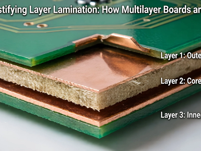
Demystifying Layer Lamination: How Multilayer Boards are BuiltJune/05/2026
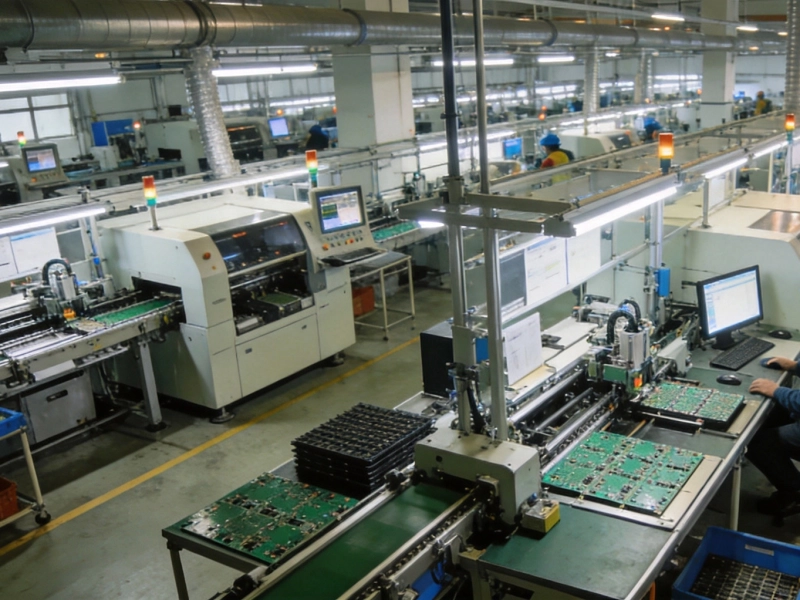
Is PCB Fabrication in China Still the Most Cost-Effective Option? A 2026 AnalysisJuly/27/2026
The Chemistry of PCB Cleaning: Why Ionic Contamination MattersSeptember/04/2026
Solder Mask and Silkscreen: More Than Just Aesthetics in the PCB ProcessJuly/20/2026

How Automation is Revolutionizing China's PCB SectorJune/03/2026
A Step-by-Step Walkthrough of the PCB Fabrication ProcessMay/21/2026
Understanding Copper Plating: Ensuring Connectivity and Durability in PCBsJuly/09/2026