Open Nav

When an Electronics Design moves beyond the realm of digital logic and enters the domain of radio frequency (RF) and microwave signals, a new set of material challenges emerges. At low frequencies, almost any PCB substrate performs adequately. At 5 GHz, 10 GHz, or 77 GHz — the frequencies used in 5G networks, automotive radar, satellite communications, and aerospace — the electrical properties of the base material become as critical as the routing geometry.
This article explains how PCB substrate materials behave at high frequencies, what material properties matter most, and how to assess and compare materials for RF and microwave applications.
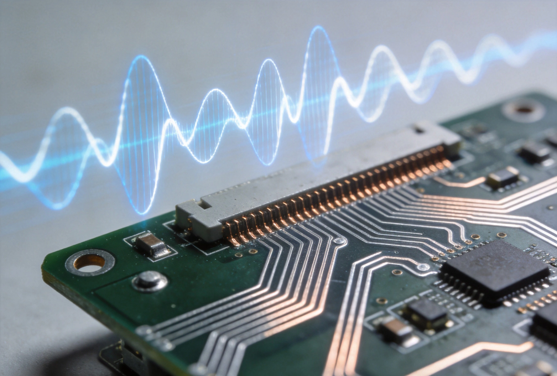
FR-4, the ubiquitous epoxy-glass composite used in the vast majority of PCBs, is optimized for cost and mechanical robustness — not electrical performance at high frequencies. Its Dielectric Constant (Dk) varies significantly with frequency, temperature, and resin content, making it unsuitable for designs where signal velocity, impedance, and loss must be controlled precisely.
Beyond Dk inconsistency, FR-4 suffers from high Loss Tangent (Df) at elevated frequencies. Signal attenuation in FR-4 at 10 GHz is roughly ten times worse than in purpose-built high-frequency laminates. For a 5G base station antenna feed network or a 77 GHz radar module, this level of loss is unacceptable — it degrades range, reduces efficiency, and generates excess heat in the substrate itself.
For RF and microwave Pcb Materials, only two electrical properties are truly fundamental:
Dielectric Constant, also called relative permittivity, determines how fast an electromagnetic wave propagates through the material. The relationship is direct: signal velocity in a dielectric is inversely proportional to the square root of Dk. A lower Dk means faster signal propagation and, for transmission lines, a given impedance requirement calls for a wider trace or larger geometry.
What makes Dk critical for microwave design is its consistency — ideally, Dk should remain flat across frequency and temperature. High-frequency laminates are engineered for stable Dk across the operating band, whereas FR-4 exhibits a Dk that falls 5–10% from 1 GHz to 10 GHz. For narrowband applications, this variation can be tuned around. For broadband systems, it creates distortion and unpredictable performance.
Common Dk values for high-frequency materials range from approximately 2.1 (PTFE at low resin content) to 10.2 (ceramic-filled substrates). Lower Dk materials suit high-speed digital and ultra-high-frequency applications; higher Dk materials are used in compact filter and antenna designs where size reduction is valued over bandwidth.
Loss Tangent, or dissipation factor (Df), quantifies how much energy a dielectric material converts to heat when an AC field passes through it. It is the primary driver of signal attenuation in the substrate. The lower the Df, the less lossy the material.
To put this in concrete terms: FR-4 has a Df of approximately 0.02 at 10 GHz — meaning it is a fairly poor insulator at microwave frequencies. A high-performance PTFE laminate might have a Df of 0.0009 at the same frequency. The difference translates directly to insertion loss: a 10 GHz transmission line on PTFE will lose roughly 20 times less power to the substrate than an equivalent line on FR-4.
For battery-powered RF devices, low Df also translates to better power efficiency and longer battery life — an increasingly important consideration in IoT sensors and mobile 5G terminals.
Polytetrafluoroethylene — the cousin of the non-stick coating on cookware — is the gold standard for ultra-low-loss microwave materials. PTFE has a Dk of approximately 2.1 and a Df below 0.001 at 10 GHz, making it ideal for applications from DC to well above 100 GHz.
The challenge with pure PTFE is mechanical: it is soft, thermally unstable during assembly (it melts around 327°C but flows at lower temperatures), and difficult to machine. Commercial PTFE PCB laminates address these issues by mixing PTFE with ceramic fillers or woven glass reinforcement. Ceramic-filled PTFE laminates like Rogers RT/duroid 6002, Rogers RO3003, and Taconic RF-35 offer significantly improved dimensional stability and thermal conductivity while maintaining excellent electrical performance.
PTFE-based boards require specialized assembly processes — they cannot be run through standard HASL (hot air solder leveling) without damage. Immersion gold (ENIG) or precision CNC milling are the preferred finish and routing methods.
Rogers Corporation is the most recognized name in high-frequency Pcb Materials, offering a broad portfolio of ceramic-filled hydrocarbon laminates under the Rogers RT/duroid, RO3000, RO4000, and TMM series.
The RO4000 series — RO4003C and RO4350B — deserves special mention because it bridges the gap between conventional and microwave materials. With Dk values of 3.3–3.5 and Df around 0.003–0.004, these materials are substantially better than FR-4 while remaining compatible with standard Pcb Fabrication processes including lead-free HASL. This has made them the de facto choice for RF power amplifiers, LNB systems, and cellular infrastructure from 1 GHz to 20 GHz.
The trade-off with RO4000 series materials is slightly higher moisture absorption than ceramic-filled PTFE. For outdoor or humid-environment designs, Rogers RT/duroid or PTFE-ceramic grades are preferred.
Materials like Isola Itera, Panasonic Megtron 6, and similar products fill a middle ground between standard FR-4 and dedicated microwave laminates. They offer Dk values around 3.5–4.5, Df in the 0.002–0.006 range, and full compatibility with standard Pcb Manufacturing equipment.
These materials are increasingly used in high-speed digital applications (26 GHz 5G fronthaul, high-speed SerDes) where the PCB also needs to support digital logic layers. The ability to use a single material system for both RF and digital functions simplifies the board stackup significantly.
For flexible or conformal RF interconnects, Polyimide films like DuPont Pyralin are used in flex and rigid-flex constructions. Polyimide has a Dk of approximately 3.5 and Df around 0.002, making it acceptable for frequencies up to approximately 20 GHz. Above that, PTFE flex becomes necessary despite its higher cost and more challenging assembly requirements.
Electrical performance is only part of the material selection equation. For production-quality RF boards, thermal and mechanical properties determine manufacturability and field reliability:
RF and microwave components — particularly power amplifiers — generate significant heat. Materials with higher thermal conductivity dissipate this heat more effectively, reducing the operating temperature of active devices and improving long-term reliability. Ceramic fillers in PTFE and hydrocarbon laminates dramatically increase thermal conductivity compared to pure polymer — a property that matters more as RF power levels increase.
TCDk measures how much the Dk changes per degree of temperature change. For narrowband RF filters and oscillators, a low TCDk is essential — a filter that drifts off frequency as the equipment warms up is not a functional product. Look for TCDk values in the ppm/°C range, and be especially critical if the data sheet does not report this parameter at all.
The coefficient of thermal expansion of the substrate must be managed relative to copper and component lead frames. A large CTE mismatch causes solder joint fatigue during thermal cycling. This is especially important for boards that experience wide temperature swings — aerospace and outdoor telecommunications equipment in particular.
Most polymer-based substrates absorb some ambient moisture. Water has a Dk of approximately 80, so even small amounts of absorbed moisture significantly change the effective Dk of a PCB substrate — particularly at microwave frequencies where sensitivity is highest. PTFE-ceramic laminates have the lowest moisture absorption, typically below 0.1%, while glass-reinforced hydrocarbon materials may absorb 0.2–0.5%.
Not all PCB manufacturers are equipped to work with high-frequency laminates. Before committing to a material, assess your manufacturing partner on the following capabilities:
Once a material is selected, the PCB stackup determines how well the board performs electrically. A few principles guide effective RF stackup design:
High-frequency materials are significantly more expensive than FR-4 — PTFE-ceramic laminates can cost 5x to 20x as much per square foot. This cost premium demands careful justification. A useful framework:
Can I use FR-4 for a 5 GHz Wi-Fi PCB?
For short traces and low-power designs, FR-4 at 5 GHz is marginal but workable. The key issue is loss — plan for approximately 0.5 dB per inch of trace length and test your return loss carefully. For anything beyond simple antenna feed-through, switch to a low-loss material.
What does "cast" vs. "calendered" PTFE mean?
Cast PTFE films are made by pressing and sintering PTFE resin, producing a very uniform dielectric constant but in limited thickness ranges. Calendered PTFE uses roller compaction and typically offers better mechanical properties at slightly less uniform Dk. For microwave PCBs, cast PTFE-ceramic composites generally deliver more consistent electrical performance.
How does frequency affect my choice of Dk?
At very high frequencies (above 20 GHz), lower Dk materials produce wider traces for a given impedance, which improves manufacturing tolerances and reduces conductor loss. At lower microwave frequencies, Dk is less critical and higher-Dk materials can be used for more compact structures. Choose the Dk that best fits your frequency range and board Size Constraints.
Do high-frequency materials require special surface finishes?
Yes. PTFE in particular is not compatible with HASL or lead-free HASL — the high temperatures and solderability issues are prohibitive. ENIG (electroless nickel immersion gold) or hard gold plating are the standard finishes for PTFE boards. Some manufacturers also use silver ink or direct bond copper (DBC) processes for specialized applications.
How do I verify the material my manufacturer used?
Request a Certificate of Conformance with material lot numbers, and cross-reference against the manufacturer's datasheet. Third-party test labs can measure Dk and Df of a finished board using the split-cylinder or differential phase length method if you need independent verification.
Heavy Copper PCBs: Capabilities for High-Current and Power ElectronicsJuly/14/2026
Minimum Trace and Space: How Far Has PCB Technology Advanced?July/01/2026

Top Trends Shaping the Chinese PCB Manufacturing Industry in 2026May/21/2026
Any-Layer Interconnect: The Pinnacle of High-Density PCB TechnologyJuly/10/2026
Large Format vs. Miniature PCBs: Evaluating Size Constraints and CapacitiesAugust/14/2026
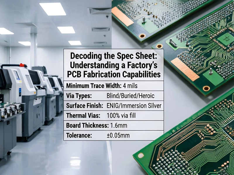
Decoding the Spec Sheet: Understanding a Factory's PCB Fabrication CapabilitiesJune/11/2026
High-Frequency Materials: Assessing Capabilities for RF and Microwave PCBsAugust/03/2026
Why Global Brands Are Turning to PCB Fabrication in China in 2026May/21/2026