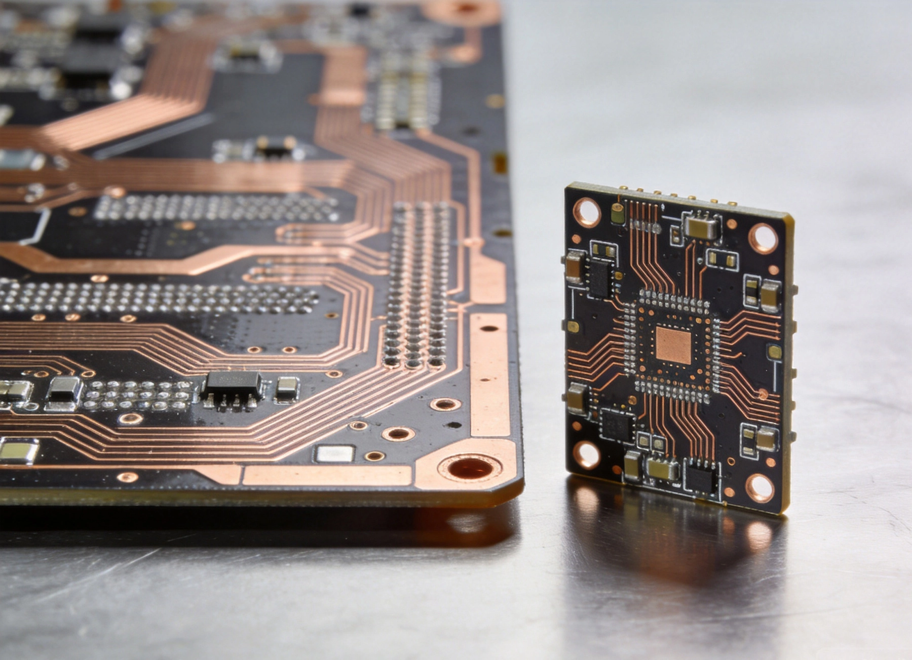
When designing electronic systems, one of the most fundamental decisions engineers face is selecting the appropriate PCB size format. The choice between large format PCBs and miniature PCBs can dramatically impact your project's cost, performance, manufacturability, and overall success. This comprehensive guide explores the critical size constraints, capacity limitations, and strategic considerations that will help you make an informed decision for your next Electronics Design.

Understanding PCB Size Categories
Printed circuit boards come in a vast range of sizes, from massive backplane panels measuring over 500mm x 500mm to ultra-compact modules smaller than a fingernail. Understanding these size categories is the first step in making the right selection for your application.
What Defines Large Format PCBs?
Large format PCBs typically measure over 300mm (12 inches) in one dimension, with some industrial applications requiring boards exceeding 600mm x 600mm. These boards are commonly found in:
- Industrial control systems and Automation equipment
- Server motherboards and telecommunications infrastructure
- Power Electronics and motor control applications
- Medical imaging devices and diagnostic equipment
- Aerospace and defense electronics
The primary advantage of large format PCBs is their ability to accommodate high component counts, complex routing, and multiple power domains in a single assembly. This reduces the need for interconnects between separate boards, potentially improving Signal Integrity and reliability.
Characteristics of Miniature PCBs
Miniature PCBs, at the other extreme, typically measure less than 100mm (4 inches) in their longest dimension, with many applications requiring boards under 50mm x 50mm. These compact boards are essential for:
- Wearable electronics and smart textiles
- IoT sensors and edge computing devices
- Medical implants and ingestible devices
- Drone electronics and autonomous systems
- Consumer electronics and mobile devices
Miniature PCBs prioritize space efficiency, often employing advanced technologies like HDI (High Density Interconnect), Microvias, and embedded components to maximize functionality within minimal footprint.
Key Size Constraints and Limitations
Both large format and miniature PCBs face unique size constraints that designers must carefully consider during the development process. These constraints affect everything from manufacturing yield to long-term reliability.
Manufacturing Limitations for Large Format Boards
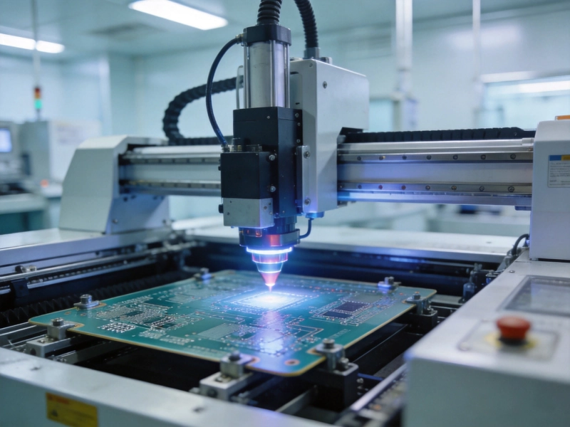
Large format PCBs present several manufacturing challenges that can impact both cost and yield:
- Panel utilization: Large boards often require specialized production panels, reducing the number of boards per panel and increasing unit cost.
- Warpage and dimensional stability: Larger boards are more susceptible to thermal warpage during manufacturing, requiring specialized handling and potentially stricter tolerance requirements.
- Layer count limitations: As board size increases, maintaining tight layer registration becomes more challenging, potentially limiting maximum layer count in some fabrications processes.
- Testing complexity: Flying Probe and bed-of-nails testing becomes more difficult and expensive on large boards, requiring custom test fixtures or multiple probe passes.
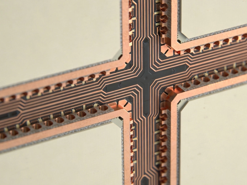
Manufacturers often charge premium rates for boards exceeding standard panel sizes (typically 18" x 24" or 457mm x 610mm), and lead times can be significantly longer due to special handling requirements.
Miniature PCB Design Constraints
Miniature PCBs face their own set of constraints that demand careful design consideration:
- Component spacing: Ipc Standards and manufacturer capabilities place minimum limits on component spacing, which can limit component density even on small boards.
- Via and trace dimensions: Smaller boards require smaller vias and traces, pushing the limits of standard fabrication processes and potentially requiring HDI technologies that increase cost.
- Thermal Management: With less surface area for heat dissipation, miniature boards require careful thermal design, potentially requiring specialized thermal vias, metal core substrates, or external heatsinking.
- Power handling: Smaller traces and planes have higher resistance, limiting current-carrying capacity and requiring careful power distribution planning.
- Assembly challenges: Smaller boards can be difficult to handle during assembly, requiring specialized fixtures and potentially increasing assembly time and cost.
Despite these constraints, advances in PCB Fabrication and assembly technology continue to push the boundaries of what's possible in miniature formats.
Capacity Considerations: Component Density and Functionality
Perhaps the most significant difference between large format and miniature PCBs is their capacity to accommodate components and functionality. This capacity directly impacts the complexity of systems that can be implemented on each board type.
Large Format PCB Capacity Advantages
Large format PCBs offer substantial capacity advantages for complex systems:
- High component count: Large boards can accommodate thousands of components, making them ideal for complex systems requiring multiple processors, memory arrays, and numerous peripheral devices.
- Multiple power domains: The abundant space allows for robust power distribution networks with multiple voltage rails, extensive filtering, and power isolation between different functional blocks.
- Complex routing: With more layers available for routing (some large format boards exceed 30 layers), complex signal routing and Impedance Control become more manageable.
- Integrated subsystems: Large boards can incorporate multiple functional subsystems (power supply, signal processing, communication interfaces, etc.) in a single assembly, reducing interconnect complexity.
- Easier testing and debugging: The additional space allows for more test points, debug interfaces, and probe access, simplifying validation and troubleshooting efforts.
Miniature PCB Capacity Optimization
While miniature PCBs have limited physical space, they can achieve remarkable functionality through careful optimization:
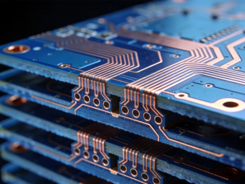
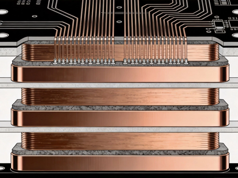
- HDI technology: Microvias, blind and Buried Vias, and sequential lamination enable multiple routing layers in a thin profile, dramatically increasing routing density.
- Component selection: Using advanced packaging (QFN, BGA, CSP) and miniature components (0201, 01005, and even smaller) maximizes component density.
- Embedded components: Embedding passive components (resistors, capacitors) within the board layers frees surface space for active components and routing.
- System-in-Package (SiP): Integrating multiple functions into a single package reduces the number of discrete components required on the board.
- Flexible and rigid-flex designs: Utilizing flexible circuits allows three-dimensional component placement, increasing effective surface area beyond the board's footprint.
Despite these optimization techniques, miniature PCBs inevitably face capacity limitations that require careful prioritization of features and functionality.
Cost Implications: Beyond Per-Unit Pricing
When comparing large format and miniature PCBs, it's essential to look beyond simple per-unit pricing and consider total cost of ownership across the entire product lifecycle.
Large Format PCB Cost Considerations
While large format PCBs typically have higher per-unit costs due to material usage and manufacturing complexity, they may offer cost advantages in other areas:
- Reduced assembly complexity: Consolidating functionality onto fewer boards reduces assembly operations, potentially lowering overall assembly cost.
- Improved reliability: Fewer board-to-board interconnects reduce potential failure points, potentially lowering warranty and field service costs.
- Easier testing: Larger boards with accessible test points can reduce testing complexity and time, improving yield and reducing scrap costs.
- Simplified Supply Chain: Fewer board types in a product reduces procurement complexity and inventory carrying costs.
However, large format PCBs also carry unique cost risks, including higher NRE (Non-Recurring Engineering) costs for tooling and test fixtures, and potentially higher material costs for large panels and special handling.
Miniature PCB Cost Factors
Miniature PCBs often have lower material costs due to smaller size, but can incur higher costs in other areas:
- Advanced fabrication costs: HDI processes, microvias, and fine features increase fabrication cost significantly compared to standard boards.
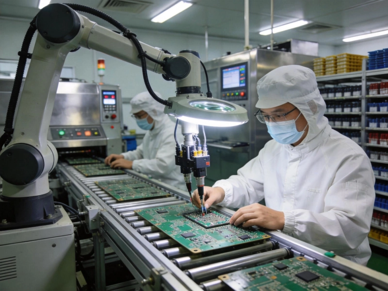
- Assembly complexity: Smaller components and tighter tolerances require more advanced (and expensive) assembly equipment and processes.
- Lower yield potential: Tighter tolerances and smaller features can reduce manufacturing yield, increasing effective per-unit cost.
- Increased testing complexity: Testing miniature boards often requires specialized fixtures and potentially more expensive X-ray Inspection for hidden connections.
- Design iteration costs: The complexity of miniature Pcb Design often requires more design iterations, increasing NRE costs.
Despite these challenges, the market trend toward miniaturization continues to drive down costs for miniature PCB technologies through improved processes and economies of scale.
Performance Trade-offs and Considerations
The choice between large format and miniature PCBs involves significant performance trade-offs that extend beyond simple size constraints. These performance considerations can impact everything from Signal Integrity to Thermal Management.
Signal Integrity Implications
Signal integrity considerations differ substantially between large and small boards:
- Large format boards: Longer trace lengths increase susceptibility to signal degradation, requiring careful Impedance Control, termination, and potentially signal conditioning. However, the additional space often allows for more robust grounding and shielding strategies.
- Miniature boards: Shorter trace lengths naturally reduce many signal integrity issues, but the close proximity of signals increases crosstalk risk. The limited space for ground planes and shielding requires more sophisticated routing strategies and potentially more expensive Pcb Materials.
Thermal Management Challenges
Thermal management presents different challenges for each format:
- Large format boards: The greater surface area facilitates heat dissipation, and the additional space allows for thermal relief structures, heatsinks, and even active cooling integration. However, power distribution across large boards can create thermal hotspots that require careful design.
- Miniature boards: Limited surface area makes heat dissipation challenging, often requiring specialized thermal materials (metal core PCBs, thermal vias), careful component placement, and sometimes external thermal management solutions. Power density becomes a critical design parameter.
Power Distribution Considerations
Power distribution design varies significantly between formats:
- Large format boards: The abundant space allows for robust power planes with minimal IR drop, multiple voltage domains with clear separation, and extensive filtering and decoupling. However, distributing power across large areas requires careful design to avoid voltage sag and ensure stable delivery.
- Miniature boards: Limited space constrains power distribution networks, often requiring creative routing, careful component placement to minimize current paths, and potentially higher-current components or external regulation. Power integrity becomes increasingly challenging at small scales.
Manufacturing and Assembly Considerations
The manufacturing and assembly processes for large format and miniature PCBs differ substantially, impacting everything from Design Rules to yield optimization strategies.
Design Rule Differences
Design Rules vary significantly between formats:
- Large format boards: Can typically accommodate more relaxed design rules (larger traces, wider spacing, larger vias) while still meeting performance requirements, potentially improving yield and reducing cost.
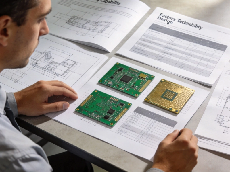
- Miniature boards: Require tighter design rules (smaller features, tighter spacing) that push fabrication capabilities to their limits, requiring careful Dfm (Design For Manufacturing) analysis and potentially more expensive fabrication processes.
Yield Optimization Strategies
Yield optimization approaches differ by format:
- Large format boards: Yield optimization focuses on panel utilization, minimizing wasted space, and designing for manufacturability with relaxed tolerances where possible. Statistical process control becomes increasingly important for large boards due to the cumulative impact of small variations across large areas.
- Miniature boards: Yield optimization requires aggressive Dfm, design for testability, and often design for assembly considerations. The high component density and small features make defect detection and correction more challenging, requiring robust inspection strategies (Aoi, X-ray, Functional Testing).
Application-Specific Recommendations
The choice between large format and miniature PCBs should ultimately be driven by your specific application requirements. Here are some general guidelines for common applications:
Choose Large Format PCBs When:
- Your system requires high component count and complex functionality
- You need multiple power domains and robust power distribution
- Signal integrity and EMI control are critical concerns
- Reliability and serviceability are important requirements
- Your application has relaxed space constraints
- You need extensive test and debug capabilities
- Cost sensitivity favors consolidated designs over miniaturized alternatives
Choose Miniature PCBs When:
- Space is at a premium (wearables, IoT, portable devices)
- Weight is a critical factor (drones, aerospace, mobile)
- Your application requires integration into small form factors
- Power requirements are modest and well-defined
- Functionality can be carefully optimized and prioritized
- You can accommodate higher per-unit costs for size advantages
- Your Supply Chain can support advanced miniature technologies
Future Trends and Emerging Technologies
The landscape of PCB size and capacity continues to evolve with emerging technologies that blur the lines between traditional categories:
- Embedded components: Increasing integration of passive and even active components within board layers enables higher density in any format.
- Additive Manufacturing: 3D printing technologies promise to revolutionize Pcb Manufacturing, enabling complex 3D structures that defy traditional size categorization.
- Flexible and stretchable electronics: New materials and processes enable PCBs that conform to non-planar surfaces, expanding design possibilities beyond rigid board constraints.
- Advanced materials: New substrate materials with improved electrical and thermal properties enable higher performance at smaller scales.
- System-in-Package integration: Continued miniaturization of SiP technology reduces the number of discrete components required, changing the equation for board size and capacity.
Conclusion
The choice between large format and miniature PCBs involves complex trade-offs between size, capacity, cost, performance, and manufacturability. There's no universal answer— the right choice depends entirely on your specific application requirements, constraints, and priorities.
Large format PCBs offer capacity, flexibility, and robustness for complex systems where space is not a limiting factor. Miniature PCBs enable the miniaturization trends driving modern electronics, allowing sophisticated functionality in remarkably small packages at the cost of increased design and manufacturing complexity.
Successful Pcb Design requires careful consideration of these factors early in the development process, with clear understanding of your requirements and realistic assessment of the trade-offs involved. By approaching the size format decision systematically and with full awareness of the implications, you can select the optimal approach for your application and set your project up for success.
Whether you're designing a massive industrial control system or a microscopic medical sensor, understanding the size constraints and capacity limitations of different PCB formats is essential for making informed design decisions that balance performance, cost, and manufacturability.
Frequently Asked Questions
Q: What is the largest PCB size that can be manufactured?
A: While theoretical maximum sizes exceed 1 meter, practical limits are typically around 600mm x 600mm for most manufacturers. Larger boards require specialized handling and may have significant cost premiums.
Q: How small can a PCB be made?
A: Miniature PCBs can be made smaller than 10mm x 10mm using advanced technologies, but practical limits are typically around 20mm x 20mm for cost-effective manufacturing. Below this size, handling and testing become increasingly challenging.
Q: Does PCB size affect signal integrity?
A: Yes, larger boards have longer trace lengths which can increase signal degradation, while smaller boards have shorter traces but more crosstalk risk due to component density. Both require careful signal integrity design.
Q: Are large format PCBs more reliable than miniature PCBs?
A: Not necessarily. Both can be highly reliable when designed properly. Large format boards may have fewer interconnects (reducing failure points), while miniature boards may have fewer components overall. Reliability depends more on design quality than size.
Q: How does PCB size affect thermal management?
A: Larger boards have more surface area for heat dissipation, while miniature boards require specialized thermal solutions. Power density becomes more critical as size decreases, requiring careful thermal design.