Open Nav

Custom PCB Fabrication bridges the gap between circuit design concepts and functional electronic products. Even experienced engineers encounter challenges when translating designs into manufacturable boards. Understanding common pitfalls enables designers to avoid costly mistakes, reduce rework cycles, and accelerate time-to-market. This comprehensive guide examines the most frequent issues encountered in custom PCB Fabrication, providing practical strategies to prevent them.

Design For Manufacturability represents the foundation of successful Pcb Fabrication. Dfm principles ensure that designs can be manufactured efficiently at target volumes while maintaining quality and cost objectives. Engineers who neglect Dfm considerations frequently encounter fabrication issues that could have been prevented through early design decisions.
Common DFM oversights include inadequate spacing between traces and pads, insufficient annular ring around via holes, and unclear specification of critical tolerances. These seemingly minor details compound during fabrication, potentially causing opens, shorts, or complete fabrication failures. Engaging with your fabrication partner early in the design process helps identify potential issues before tooling commitments.
Most fabricators publish design guidelines specifying minimum capabilities for trace widths, spacing, drill sizes, and other parameters. These guidelines reflect actual manufacturing tolerances and should inform design decisions. Treating these specifications as absolute minimums rather than comfortable targets provides margin against process variation.
Trace width violations rank among the most common reasons for fabrication delays or rejections. Designers sometimes specify trace widths that fall below manufacturer capabilities, particularly for fine-pitch components or High-density Interconnect designs. When fabricators cannot reliably produce these traces, projects stall while designers scramble to modify layouts.
Internal copper traces face additional constraints compared to outer layers. fabrication processes introduce more variation in inner layer features due to lamination and etching exposures. Conservative designers maintain wider inner layer traces than outer layer equivalents for equivalent current carrying capacity. This margin accommodates process variation while ensuring reliable yield.
Spacing between traces and other features requires equal attention. Minimum spacing violations create short circuits during fabrication or testing. However, spacing must also accommodate fabricator registration tolerances. Designs with features approaching spacing minimums risk failures when layer-to-layer registration shifts slightly during lamination.
Annular ring—the copper pad surrounding a drilled via—determines mechanical reliability and electrical connectivity. Insufficient annular ring causes drill breakout, where the drill hole removes excessive pad copper and compromises connection integrity. This failure mode might pass automated optical inspection but fail during thermal cycling or mechanical stress testing.
Industry guidelines recommend minimum annular ring of 0.005 inches (5 mils) for standard vias, with larger values for higher reliability applications. Blind and Buried Vias require even larger annular rings due to registration challenges during sequential lamination. Designers specifying ultra-small vias must balance miniaturization goals against manufacturing realities.
Via-in-pad designs—where component leads connect directly to via barrels—require special consideration. Standard plating processes cannot reliably plate via barrels when pads connect directly to component mounting surfaces. Specialized processes like plug-and-plate or filled vias add cost but enable reliable Via-in-pad designs. Understanding these tradeoffs early prevents unpleasant surprises during fabrication.
Rf and high-speed digital designs frequently require Controlled Impedance traces to maintain Signal Integrity. Achieving consistent impedance across fabrication batches demands precise stackup control, material consistency, and process monitoring. Designers who specify impedance requirements without providing complete stackup information often receive boards that fail to meet targets.
Critical parameters for Impedance Control include substrate thickness, Dielectric Constant, trace width, and copper thickness. Each of these parameters has tolerance ranges that affect final impedance. A complete impedance specification should include tolerance requirements (typically ±10% or tighter), which determines acceptable parameter variation ranges.
Material selection significantly influences impedance consistency. Standard FR-4 materials exhibit Dielectric Constant variation of ±10% between batches, affecting impedance by corresponding amounts. High-frequency laminates like Rogers or Panasonic Megtron provide tighter dielectric constant tolerances but at substantially higher cost. Matching material specifications to actual performance requirements prevents unnecessary expense while ensuring adequate control.
Power Electronics and high-current designs generate significant heat that must dissipate through the PCB. Inadequate thermal design causes premature component failure, intermittent operation, or complete system shutdown. Thermal management should integrate into the Pcb Design from initial concept rather than being added as an afterthought.
Thermal vias transfer heat from component pads to internal planes or external heatsinks. Via arrays surrounding power components create thermal paths with resistance measured in degrees Celsius per watt. Designers should calculate thermal resistance based on actual component power dissipation and acceptable temperature rise. Underestimating thermal requirements leads to field failures that damage product reputation.
Copper weight selection affects both current capacity and thermal performance. Heavy copper provides lower resistance for high-current paths while also improving heat spreading. However, heavy copper introduces challenges in plating, etching, and Solderability. Fabricators capabilities for heavy copper vary significantly, making early supplier consultation essential for high-power designs.
Component pad dimensions directly influence assembly reliability and fabrication yield. Pads too small cause tombstoning, insufficient solder, and poor solder wetting. Excessive pad size promotes bridging between adjacent pads, particularly for fine-pitch components. Finding optimal pad dimensions balances these competing requirements.
Thermal relief patterns connect pads to internal planes while facilitating solder flow during assembly. Pads connected directly to large copper planes experience reduced Solderability due to thermal shunting. The heat sinking effect draws heat away from the joint faster than solder can reflow, resulting in cold joints or incomplete connections. Proper thermal relief geometry maintains thermal isolation while preserving electrical connectivity.
Surface finish selection affects long-term solderability and shelf life. Hasl (Hot Air Solder Leveling) provides adequate solderability but introduces uneven surfaces unsuitable for fine-pitch components. Enig (Electroless Nickel Immersion Gold) offers flat surfaces and excellent shelf life but presents risk of black pad syndrome if process control lapses. Osp (Organic Solderability Preservatives) provides cost-effective protection for immediate assembly but degrades rapidly after exposure.
Incomplete or ambiguous fabrication documentation causes more delays than technical limitations. Gerbers without board outlines, drill files missing tooling notes, and stackup specifications lacking tolerance information force fabricators to request clarification. These interruptions extend lead times and introduce communication errors that compromise quality.
Standard fabrication drawing requirements include board dimensions with tolerances, drill chart with plating specifications, layer stackup with material designations, surface finish requirements, and Silkscreen specifications. Drawings should explicitly state any non-standard requirements or unique quality expectations. Ambiguity benefits no party—clarity accelerates fabrication and ensures expectations align.
Testing and inspection requirements deserve explicit documentation. IPC Class 2 represents standard commercial requirements while IPC Class 3 addresses high-reliability applications. Beyond class designation, specific test requirements like impedance testing, microsection analysis, or burn-in should appear in fabrication specifications. Without clear requirements, fabricators apply standard inspection criteria that might miss application-specific concerns.
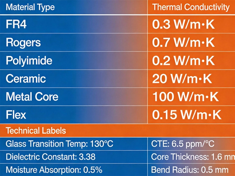
PCB substrate materials influence electrical performance, thermal behavior, and fabrication compatibility. Standard FR-4 serves many applications adequately but reaches limitations for elevated temperature, high-frequency, or demanding mechanical environments. Engineers who specify inappropriate materials encounter failures that seem mysterious until root cause analysis identifies material incompatibility.
Tg (glass transition temperature) specifies the temperature where substrate changes from rigid to rubbery state. Designs operating near maximum-rated temperatures with limited thermal margin risk dimensional instability. High-Tg materials (170°C and above) provide improved thermal margins for elevated temperature applications, though at higher cost and potentially reduced processability.
High-frequency applications require laminates with controlled dielectric constant and low Loss Tangent. Standard FR-4 exhibits Loss Tangent increasing with frequency, causing signal attenuation unsuitable for RF designs. Rogers and similar high-frequency materials maintain stable electrical properties through microwave frequencies but require specialized processing that increases cost and lead time.
Fabrication quality verification prevents defective boards from reaching assembly or field deployment. Appropriate testing levels depend on application criticality and failure consequence. A single defective Prototype costs primarily in delay and rework expense. Field failures in medical devices or safety systems carry reputation damage, liability exposure, and potential regulatory consequences.
Basic Electrical Testing verifies continuity and isolation for all nets. Bed-of-nails fixtures or Flying Probe testers identify shorts, opens, and spacing violations. Flying Probe offers flexibility for Prototype quantities while fixture testing provides faster throughput for production volumes. All boards should receive some form of electrical verification before assembly.
Advanced testing applies to critical applications. X-ray Inspection reveals hidden defects in ball grid arrays and other bottom-terminated packages. Microsection analysis verifies plating quality, via integrity, and dielectric consistency. These destructive or time-intensive tests apply to qualification samples and periodic process monitoring rather than every board.
Fabrication partner capabilities vary dramatically across the industry. Domestic and international fabricators offer different combinations of capability, cost, and service. Matching partner capabilities to application requirements optimizes overall value rather than optimizing single variables like lowest price.
Communication quality significantly influences project outcomes. Partners who proactively communicate challenges, suggest improvements, and provide realistic lead times generate better results than those who accept orders without engagement. Early discussion of challenging requirements allows partners to prepare appropriate processes rather than encountering surprises during fabrication.
Documentation sharing builds partnership effectiveness. Providing complete design files, stackup information, and quality expectations gives fabricators the information needed to succeed. Treating fabrication as a transactional commodity exchange rather than collaborative engineering relationship misses opportunities for Design Optimization and risk reduction.
Custom Pcb fabrication success depends on designer knowledge, clear communication, and appropriate expectations. Common pitfalls in trace design, Impedance Control, thermal management, and documentation frequently cause delays, cost overruns, and quality issues. Understanding these challenges enables designers to avoid predictable mistakes and achieve better outcomes.
The most successful approaches treat fabrication partners as collaborative resources rather than anonymous suppliers. Early engagement, clear documentation, and responsive communication prevent most issues before they materialize. When problems do arise, established relationships facilitate rapid resolution rather than finger-pointing and delays.
Investing time in Dfm Review, material selection, and specification clarity pays dividends through faster delivery, lower cost, and improved quality. These upfront investments cost far less than fabrication failures, field returns, or project delays. Your fabrication partner can provide guidance—but only if you engage them early and provide the information needed to help.
Exploring Special Materials in Custom PCB FabricationMay/21/2026

The Rise of Smart Factories: How Automation is Revolutionizing China's PCB SectorJune/16/2026

Overcoming Language and Cultural Barriers in Chinese PCB SourcingJuly/07/2026

Rigid-Flex and Flexible PCBs: Unlocking New Possibilities with Custom DesignsJuly/17/2026

Understanding Lead Times: What to Expect When Ordering from Chinese PCB MillsAugust/06/2026

Environmental Standards in China: How PCB Factories are Going GreenSeptember/11/2026
Essential Tips for Your First Custom PCB OrderJune/02/2026

A Complete Guide to Importing Custom PCBs from China for US and EU StartupsJuly/16/2026