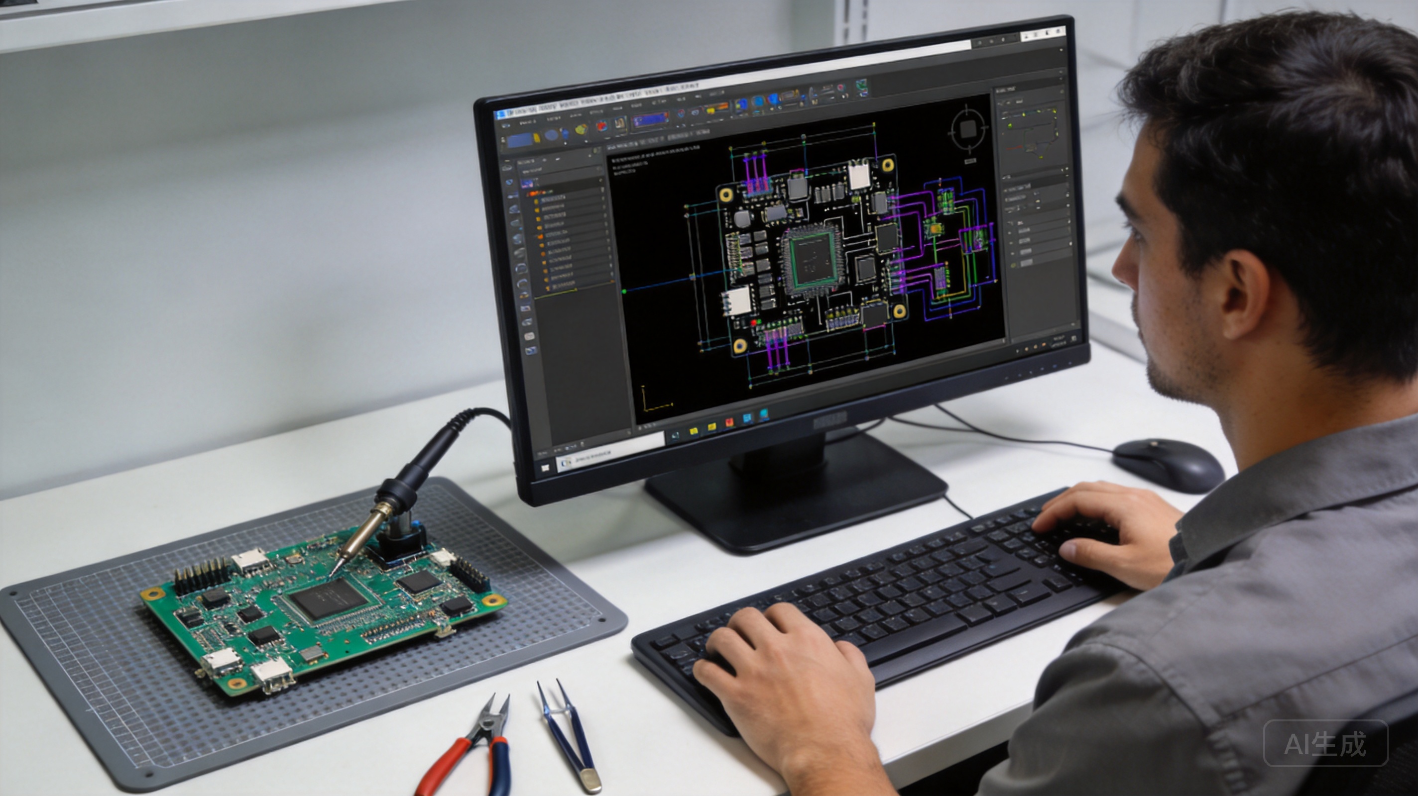
Designing your first Custom Pcb order is an exciting milestone in any electronics project. Whether you're creating a Prototype for a startup product, building a hobby project, or developing an industrial control system, the transition from schematic to physical board brings both challenges and rewards. A well-designed PCB can function reliably for years, while a poorly planned design can lead to frustrating delays, costly re-spins, and sleepless nights debugging mysterious failures.
The difference between success and failure often comes down to understanding the manufacturing process and designing with producibility in mind. This guide provides essential tips that will help you navigate your first Custom Pcb order with confidence, avoiding common pitfalls that catch many first-time designers.
Before opening your CAD software, take time to define what you're actually building. Clear specifications prevent misunderstandings and ensure your final board meets expectations.
Create a specification document that answers these fundamental questions:
Writing these down before you start designing forces you to think through critical decisions early, when changes are inexpensive, rather than later when reworking the design becomes costly.
Your first custom PCB should prioritize simplicity over feature density. Building a complex board with dozens of components and dense routing increases the chance of problems. Start with a straightforward design that proves out your core functionality before adding advanced features.
Selecting the appropriate board type for your application forms the foundation of a successful design. Different PCB types offer different capabilities and trade-offs.
The number of layers directly affects cost, complexity, and routing flexibility:
For your first PCB, consider starting with single or double-sided unless your design absolutely requires more layers. The additional complexity of multi-layer boards brings tighter tolerances and more potential failure points.
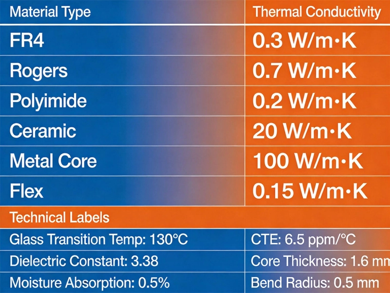
Most standard PCBs use FR-4, a fiberglass-epoxy composite that offers good general-purpose performance at reasonable cost. For specialized applications, consider:
Unless your application has specific material requirements, stick with standard FR-4. It's well-understood, easy to work with, and available from virtually all manufacturers.
Design rules define the physical constraints that your manufacturer can reliably produce. These aren't arbitrary limitations—they represent real-world Manufacturing Capabilities and tolerances.
Every manufacturing process has inherent limitations. A drill bit cannot create holes smaller than its diameter. An etching tank cannot reliably produce traces narrower than a certain width. By designing within these constraints, you ensure your boards can be produced consistently and reliably.
Designing outside design rules doesn't just risk rejection—it risks marginal boards that pass inspection but fail in the field. Save yourself the trouble and design within spec from the start.
Your design rules should address these critical parameters:
Always obtain design rules from your specific manufacturer before finalizing your layout. Generic design rules found online may not match your chosen partner's actual capabilities. Most reputable manufacturers provide:
When in doubt, ask your manufacturer directly. Their engineering team can clarify capabilities and may be able to accommodate borderline requirements with appropriate cost and lead-time adjustments.
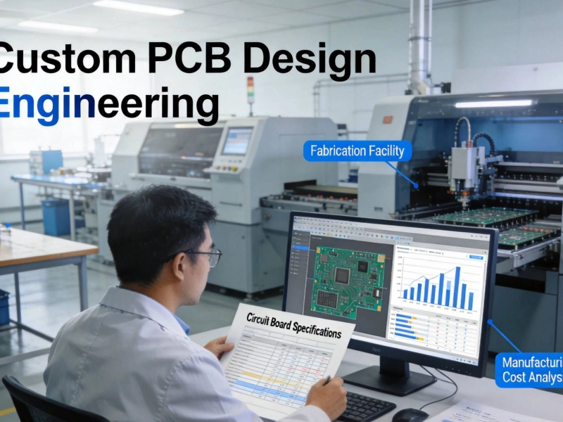
Your CAD software produces the design, but you need to generate specific manufacturing files for your PCB fabricator. Understanding these files prevents miscommunication and ensures your board is built correctly.
Gerber Files are the universal format for Pcb Manufacturing. Each Gerber file describes one layer of the board:
Always verify your Gerber Files before sending them out. Many CAD programs have built-in Gerber viewers; free tools like GerberViewer also exist. Double-check that all layers are present, properly sized, and aligned.
Drill files specify hole locations, sizes, and plating requirements. The most common format is Excellon (NC Drill). Your drill file should include:
Verify that your drill file coordinates match your Gerber files. Mismatched files are a common source of problems.
Beyond the manufacturing files, provide:
Even the clearest files benefit from good communication with your manufacturer. Establishing a clear dialogue prevents misunderstandings and ensures your expectations are understood.
Surface finish affects solderability, shelf life, and cost. Common options include:
Discuss these options with your manufacturer to select the best finish for your assembly process and application.
Manufacturing involves many steps, each with its own tolerances. Understanding how these tolerances stack up helps you set realistic expectations:
Your manufacturer can help you understand these trade-offs and adjust designs to maximize yield while meeting your requirements.
Learning from others' mistakes saves time and money. Here are the most common issues that catch first-time PCB designers.
Traces too close together create solder bridges and assembly problems. Traces too close to the board edge risk delamination during depanelization. Always verify clearances before releasing files for manufacturing. Use your design rule check (DRC) function and then visually inspect the results.
Silkscreen markings often get overlooked until assembly reveals confusing component placement. Include clear reference designators, polarity indicators, and connector pinouts on the silkscreen. These markings save significant time during assembly and debugging.
For fine-pitch components, consider using solder mask defined (SMD) pads rather than copper defined. SMD pads provide a smaller opening surrounded by solder mask, reducing the risk of solder bridges during assembly.
How will your boards be separated from the manufacturing panel? V-scoring works for straight cuts, while mouse bites require routing. Your manufacturer needs to know your depanelization method to plan the panel properly. Include mouse bite tab locations and sizes if applicable.
Adding test points to your design enables efficient electrical testing. Consider adding:
Test points cost almost nothing to add during design but become invaluable during assembly verification and debugging.
Your schematic assumes ideal components, but actual components have tolerances. When designing analog circuits, consider how component variation affects circuit behavior. Design with appropriate tolerance bands and consider corner-case scenarios during simulation.
Even perfectly designed PCBs benefit from quality verification. Testing catches manufacturing defects before they cause assembly failures or field returns.
Start with a careful visual inspection under magnification. Look for:
Request manufacturing continuity and isolation testing from your fabricator. This automated test verifies:
For more thorough verification, consider flying probe testing or in-circuit testing during assembly.
For critical applications or first-time designs with a new manufacturer, request a cross-section analysis. This destructive test reveals:
Understanding the physical characteristics of your boards builds confidence in the manufacturing process.
Your Pcb Manufacturer is a partner, not just a vendor. Building a good relationship improves communication, enables collaboration on challenging designs, and often results in better pricing and service over time.
Begin your relationship with a prototype order. This initial order lets you:
Once you've validated the relationship with a successful prototype, scaling to production quantities becomes much smoother.
When issues arise, provide specific, constructive feedback rather than just complaints. Help your manufacturer understand what went wrong, what impact it had, and what you'd like to see improved. Most quality-focused manufacturers appreciate the opportunity to resolve issues and prevent recurrence.
PCB manufacturers have specialized knowledge about producibility, materials, and processes. When they suggest design changes, listen carefully—they're trying to help you avoid problems. Their experience with thousands of designs provides valuable insights that can improve your boards.
Designing your first custom PCB order doesn't have to be intimidating. By following these essential tips—starting with clear specifications, understanding Manufacturing Capabilities, communicating effectively with your chosen partner, and learning from common mistakes—you'll set yourself up for success.
Remember that Pcb Design is both art and science. The technical aspects (design rules, file formats, stack-ups) can be learned from documentation and tutorials. The intuitive understanding of what makes a design "clean" and producible comes from experience. Give yourself permission to learn, and don't be discouraged if your first design requires revisions.
The most successful PCB designers treat their fabricator as a partner. Engage them early, ask questions freely, and build a relationship that benefits both parties over time. With each project, you'll gain confidence and expertise that makes the next design easier.
Your first custom PCB order represents the beginning of an exciting journey into electronics development. Embrace the learning process, apply the principles in this guide, and watch as your ideas transform from schematics into physical reality.
Costs vary widely based on board specifications. Simple single-sided boards may cost $5-20 for prototype quantities, while complex multi-layer boards with advanced materials can cost hundreds or thousands of dollars. Most fabricators provide online instant quotes based on specifications like size, layers, quantity, and materials. Expect lower per-unit costs at higher volumes due to fixed setup costs being distributed across more boards.
Prototype lead times typically range from 3-7 business days for standard specifications, with expedited options available for premium pricing. Multi-layer boards and specialized materials may require 10-15 days or longer. Production quantities often have similar or slightly longer lead times per batch, though larger orders may require scheduling coordination.
Yes, most manufacturers accept single-piece orders, though the per-unit cost is significantly higher than for batch production. Some offer low-cost prototype programs specifically designed for engineers testing new designs. Consider pooling multiple designs into a single order if you have several projects to prototype, as this reduces per-board cost.
At minimum, provide Gerber files for all copper layers, solder mask, and silkscreen, plus an Excellon drill file. A board outline file is also typically required. Many manufacturers also accept the native CAD file format from popular tools like Eagle, KiCad, Altium, and others, which simplifies the process and reduces file conversion errors.
Run your CAD software's design rule check (DRC) against your manufacturer's specific design rules. This automated check identifies most violations. Additionally, send your files to the manufacturer for a professional design review before ordering—most reputable manufacturers offer this service free or for a nominal fee. They can identify potential issues and suggest modifications that improve manufacturability.
The Economics of Customization: Balancing Performance and Budget in PCB DesignJune/17/2026

Rigid-Flex and Flexible PCBs: Unlocking New Possibilities with Custom DesignsJuly/17/2026

From Prototype to Mass Production: Scaling Your Custom PCB Project SeamlesslyJuly/07/2026

The Rise of Smart Factories: How Automation is Revolutionizing China's PCB SectorJune/16/2026

A Complete Guide to Importing Custom PCBs from China for US and EU StartupsJuly/16/2026

Overcoming Language and Cultural Barriers in Chinese PCB SourcingJuly/07/2026
Exploring Special Materials in Custom PCB FabricationMay/21/2026

24-Hour Turnaround: Is it Possible and How Does it Work?May/21/2026