Open Nav

The relentless drive toward smaller, lighter, and more capable electronic devices has forced PCB designers to push beyond the limitations of conventional through-hole and Multilayer Board technology. In the consumer electronics that fill pockets and backpacks worldwide — smartphones, tablets, wearables — the printed circuit board inside is doing more work in less space than ever before. The technology that makes this possible is called HDI, or High Density Interconnect, and its core enabling technologies are microvias and blind and buried via structures. Understanding these technologies is essential for anyone designing or sourcing boards for modern compact electronics.
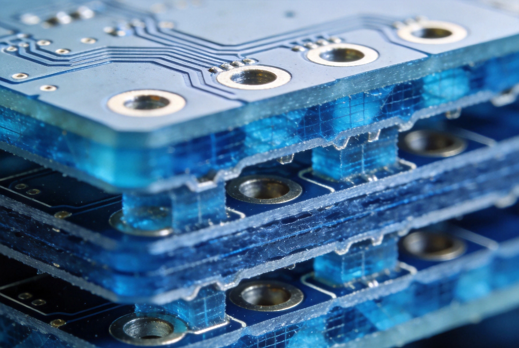
HDI refers to a class of PCB designs that achieve higher wiring density than conventional boards through finer line widths and spacings, higher pad densities, and more efficient use of board real estate through Microvia and blind/buried via technology. The IPC-2315 standard defines HDI by board complexity metrics, but the practical definition is simpler: an HDI board is one where the routing density — measured by the ratio of routing area to total board area — significantly exceeds what is achievable with standard through-hole technology.
The primary driver of HDI adoption is miniaturization. Every generation of smartphone, smartwatch, and hearing aid pushes the envelope on how many components can be placed in a given area. Surface Mount components continue to shrink — 01005 is now routine, 008004 is entering production — and routing traces between those components requires density that through-hole vias simply cannot provide efficiently. Microvias and blind/buried structures solve this by connecting only the layers that need to be connected, without consuming space on every layer of the stack-up.
A Microvia is a via with a diameter of 0.15 mm (6 mil) or smaller, typically formed by Laser Drilling rather than mechanical drilling. The Laser Drilling process creates a precise, small-diameter hole that can be placed with high accuracy, making it suitable for fine-pitch component pad escape routing and layer-to-layer interconnections in high-density areas.
The most common type of microvia is the staggered microvia, where microvias on adjacent layers are offset from each other, connected by a trace segment in the plane between them. This is sometimes called a skip-via or stitched via architecture. A microvia on layer one connects to a trace on layer two, which connects to a microvia on layer three, and so on. The layer-count penalty for a microvia is typically one or two layers per connection rather than the full board thickness of a through-hole via.
Stacked microvias take this further by placing microvias directly on top of each other across consecutive layers. This requires more precise laser ablation and plating processes and is more expensive to manufacture, but it allows for the highest routing densities and is commonly found in chip-on-board and package-on-package (PoP) applications where vertical integration is paramount.
The aspect ratio of a microvia — the ratio of depth to diameter — is typically kept below 1:1 or at most 1:1.5 to ensure reliable plating. A microvia that is 0.1 mm in diameter should be no more than 0.15 mm deep to achieve uniform copper plating on the barrel walls. This depth constraint means microvias are inherently suited to connecting adjacent layers rather than spanning large distances through the board stack.
A blind via is a hole that starts at one surface of the board and connects to one or more inner layers, but does not penetrate through to the opposite surface. It is "blind" because you cannot see through it from either face of the board. Blind vias are typically created by drilling and plating before the full board stack is laminated, or by using controlled depth laser drilling after lamination.
The key advantage of blind vias is that they preserve routing space on layers that are not part of the connection. A blind via from the top layer to layer three, for instance, does not consume pad land on layer two or on the bottom of the board. This space saving is critical in high-density areas near BGA packages and other fine-pitch components where routing channels are scarce.
Blind vias can be manufactured in several ways. Sequential lamination — where some inner layers are built up and cured before subsequent layers are added — is one approach. The hole is drilled into the partially completed stack, plated, and then more layers are built on top. Laser drilling from one side through the outer dielectric layer is another common method, particularly effective for thin dielectric layers in HDI boards. Controlled depth laser ablation, where the laser stops at a defined copper land on the target layer, is also widely used.
A buried via is an interconnection between inner layers that is not visible from either board surface. It exists entirely within the board stack, connecting layers that are internal to the stack-up. Buried vias are created during the sequential lamination process: inner-layer pairs are drilled, plated, and laminated together, and then the full board build-up proceeds around that core.
Buried vias are particularly useful in designs with high layer counts where routing between internal planes is needed but surface layer density must be preserved. Complex telecommunications infrastructure boards, advanced computing boards, and military-grade electronics routinely use buried via structures to manage routing complexity without expanding board dimensions.
The manufacturing challenge with buried vias is that any buried connection must be made before the final board stack is complete. This means that buried via layers are essentially fixed once laminated. Design changes that require modifying a buried via layer are extremely costly and often impractical after the inner cores are bonded. This makes thorough design verification before manufacturing particularly critical for boards that rely heavily on buried via structures.
HDI boards with microvias and blind/buried vias require carefully planned stack-up sequences that account for the order in which each layer and each via structure will be created. The stack-up sequence determines which layers can connect to which others, how thick each dielectric layer must be, and how many lamination cycles the board will require.
A typical 8-layer HDI board with microvia and blind via technology might use a sequence like this: the inner four layers are built as a core, with buried vias connecting specific combinations of those layers. The outer two layers are then built up with dielectric and copper, and blind vias are laser-drilled through the outer dielectric to connect the surface layers to selected inner layers. Microvia arrays fan out from BGA pads on the surface into the inner routing layers. The result is a board where the effective interconnect density far exceeds what a conventional 8-layer through-hole board could achieve.
The number of lamination cycles a board goes through has a significant impact on manufacturing cost and yield. Each additional lamination cycle adds processing time, material cost, and some risk of delamination or dimensional change. HDI designs that can achieve their routing objectives within two or three lamination cycles are generally more manufacturable and cost-effective than those requiring four or more.
Designing with microvia and blind/buried via technology requires adhering to manufacturer-specific Design Rules that are stricter than conventional through-hole rules. The most important constraints to understand are minimum hole size, minimum capture pad diameter, minimum land width, and spacing rules between adjacent via structures.
For laser-drilled microvias, minimum finished hole diameters typically range from 0.075 mm to 0.15 mm depending on the fabricator's equipment and process capability. The capture pad on the layer being connected should be at least 0.2 mm in diameter for reliable plating and registration, and most designers use 0.25 mm or larger to provide manufacturing margin. The annular ring — the copper land width around the finished hole — should be at least 0.05 mm on all sides to ensure the plated barrel is fully contained within the pad after registration tolerance is accounted for.
Blind via Design Rules vary by the method used to create them. Laser-drilled blind vias typically have minimum depth constraints based on the dielectric thickness. For sequential lamination blind vias, the depth is naturally limited by the stack-up, but registration between the blind via and the underlying target pad must be carefully controlled across multiple lamination cycles. Buried via design rules are typically the most forgiving since both sides of the buried connection are processed simultaneously within the same inner-layer core.
Microvias and blind/buried vias in HDI boards are subject to thermal cycling stresses that differ from conventional through-hole vias. Because microvias are typically small and shallow, they generally exhibit good thermal fatigue resistance — the small copper barrel experiences less stress per thermal cycle than a deep through-hole barrel. However, stacked microvia architectures, where microvias are placed directly on top of copper lands that themselves contain filled microvias below, can create stress concentration points that merit careful reliability analysis.
Blind and buried vias introduce interface boundaries between differently processed layers into the board cross-section. During thermal cycling, these interfaces can experience differential expansion that creates localized stress. The quality of the lamination bond between layers is the primary determinant of long-term reliability at these interfaces. Boards built with high-Tg materials and controlled lamination profiles generally perform better in thermal cycling environments.
For high-reliability applications such as automotive under-hood electronics or aerospace systems, designers should specify thermal cycling testing to the appropriate standard — IPC-6012 for Class 3 automotive, or the applicable MIL-PRF spec for defense applications — to validate the blind and buried via structures for the specific environment.
The cost of HDI boards scales significantly with the complexity of their via architecture. Simple two-layer boards with microvia fan-out from BGA pads are moderately more expensive than equivalent conventional boards — typically 20 to 50 percent more depending on the density and layer count. Boards with multiple blind via layers and buried via structures can cost two to five times their conventional equivalents, primarily driven by the additional lamination cycles, laser drilling time, and sequential processing steps required.
The most significant cost driver is often the number of lamination cycles, followed by the total number of laser-drilled holes. Designers can manage costs by minimizing the number of blind and buried via layers, using staggered microvia routing rather than stacked microvias where the routing can tolerate the additional layer offset, and consolidating routing into the minimum number of layers necessary to achieve the required interconnect density.
The primary application driving microvia and blind/buried via technology is consumer mobile electronics — smartphones, tablets, and wearables — where board area is at a premium and every square millimeter of real estate has measurable value. The PoP architecture used in many mobile processors uses stacked microvias to connect memory packages directly on top of processor packages, eliminating the need for routing between them on the board surface.
Beyond consumer electronics, HDI via technology is increasingly common in medical electronics where miniaturization enables less invasive implants and portable diagnostic devices, in automotive electronics for advanced driver assistance systems and infotainment, and in high-frequency communications infrastructure where Controlled Impedance routing and consistent via stub lengths are critical for Signal Integrity.
Microvias and blind/buried via structures are the foundational technologies of modern HDI PCB Fabrication. They enable routing densities that conventional through-hole technology cannot achieve, allowing designers to pack more functionality into smaller form factors while maintaining Signal Integrity and manufacturing yield. Successful use of these technologies requires careful attention to design rules specific to each via type, stack-up planning that accounts for manufacturing sequence, and an honest evaluation of the cost and reliability implications of increasing via complexity. For designers working on compact, high-performance products, understanding these technologies is no longer optional — it is a core competency.
How to Specify Tolerances and Stack-ups for High-Precision Custom PCBsJuly/28/2026

Questions to Ask Before Placing a Rush Order for PCB FabricationSeptember/15/2026
Custom Surface Finishes: Choosing Between ENIG, HASL, OSP, and Immersion SilverSeptember/14/2026

How AI-Driven Scheduling is Making Rapid PCB Prototyping More ReliableJune/18/2026

Thermal Management Strategies for Dense Multilayer PCB DesignsJuly/31/2026

Comparing Traditional vs. Digital Quick Turn PCB ServicesJuly/18/2026
Best Practices for Preparing Files for Expedited PCB ManufacturingJuly/29/2026

Emergency PCB Runs: Strategies for Getting Boards Fast Without Sacrificing ReliabilityJuly/08/2026