
Dense multilayer printed circuit boards push the boundaries of Electronics Miniaturization. Fitting more functionality into smaller form factors creates significant thermal challenges that designers must address early in the development process. Heat buildup in compact assemblies degrades component reliability, reduces performance, and can cause premature failure. Understanding Thermal Management strategies becomes essential for anyone working with modern high-density PCB designs.
This article explores proven techniques for managing heat in Multilayer Boards, from material selection to thermal via implementation. Whether you are designing server blades, compact power converters, or high-performance consumer electronics, these strategies help ensure your designs perform reliably over their intended lifetime.
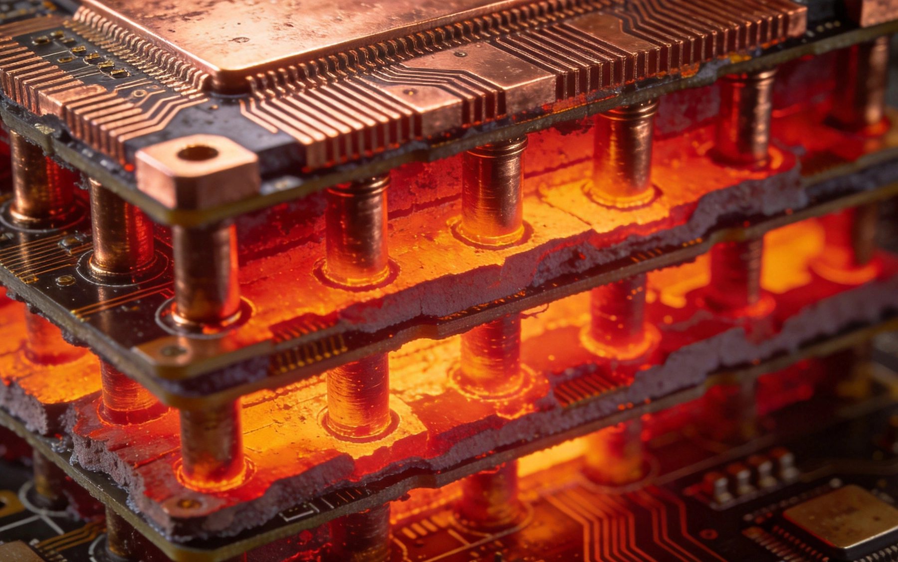
Multilayer PCBs naturally trap heat because the board structure inhibits heat flow away from active components. Unlike single-sided assemblies where components can mount directly to metal enclosures or heat sinks, multilayer designs often locate hot components in board interiors or under other components. This thermal isolation makes heat removal significantly more difficult.
The situation intensifies as component density increases. Modern processors, FPGAs, and power management ICs dissipate substantial power in compact packages. When dozens of these components occupy a small board area, the combined heat output creates thermal densities that exceed what passive cooling can handle without explicit design attention.
Heat moves through PCB structures through three mechanisms: conduction through materials, convection from surfaces, and radiation at higher temperatures. Of these, conduction dominates within the board structure while convection handles heat removal from board surfaces. Effective Thermal Management addresses both stages of heat flow.
Pcb Materials have relatively poor thermal conductivity compared to metals. Standard FR-4 laminate conducts heat at approximately 0.3 W/(m·K), while metal core substrates might reach 200 W/(m·K) or more. This thousand-fold difference means that heat spreading through PCB material happens slowly, creating temperature gradients that stress components and solder joints.
Dense multilayer designs face compounding thermal challenges. First, high component density concentrates heat sources in limited areas. Second, routing constraints often prevent placing thermal vias under all heat-generating components. Third, the board may need to operate in environments with limited airflow or elevated ambient temperatures.
Component miniaturization worsens these problems. Smaller packages have less surface area for heat dissipation and typically connect to the board through fewer and smaller leads. Ball grid array packages, commonly used for dense designs, rely almost entirely on thermal vias through the board for heat removal, making thermal via design critical.
Thermal vias provide the primary path for heat conduction from component pads through the PCB to heat-spreading layers or external heat sinks. A properly designed thermal via array can dramatically improve heat transfer efficiency, reducing component junction temperatures by tens of degrees in demanding applications.
The basic principle involves creating low-resistance thermal paths from heat sources to copper planes or external surfaces where convection can remove heat. Thermal vias accomplish this by filling or plating via barrels with high-conductivity copper, creating direct metal pathways through the low-conductivity PCB material.
Thermal via effectiveness depends on several geometric factors. Via diameter affects both thermal resistance and manufacturing cost. Smaller vias can be placed more densely but conduct less heat per via. Larger vias conduct better but consume more board area and may interfere with routing. Typical thermal via diameters range from 0.3mm to 0.5mm, balancing thermal performance with practical constraints.
Via length matters because heat must conduct through the entire board thickness. For thermal vias to work effectively, they should connect directly to copper planes on multiple layers, creating short conduction paths. Via depth that terminates in buried or blind layers wastes thermal conductivity because the heat must still travel through remaining laminate to reach external surfaces.
Thermal via arrays typically contain between 4 and 64 vias under a component, depending on thermal requirements and available space. The pattern distribution matters as much as total count. Concentrating vias near the component center where heat generation is highest produces better results than uniform spacing.
Thermal via land diameter should be larger than the barrel to provide adequate copper plating and可靠的 connection to component pads. Typical land diameters range from 0.6mm to 0.9mm for 0.3mm to 0.5mm barrel diameters. The copper plating thickness in thermal vias should be maximized within Manufacturing Capabilities, typically 25-50 micrometers, to maximize thermal conductivity.
Copper planes in Multilayer Boards provide excellent heat spreading because copper has thermal conductivity approximately 500 times greater than FR-4. Strategic placement of copper directly under or adjacent to heat sources allows heat to spread across a larger area before conducting through the board or reaching external surfaces.
Effective heat spreading requires copper planes with sufficient area and thickness. Thin copper layers, while adequate for electrical purposes, provide limited thermal benefit. Heavy copper planes of 2-ounce or 3-ounce copper dramatically improve thermal performance but increase board cost and weight. The trade-off requires careful analysis based on thermal requirements and budget constraints.
Locating copper thermal planes close to heat-generating components maximizes their effectiveness. For bottom-side components, the nearest internal layer provides the shortest thermal path. For top-side components, the first internal layer or a thermal via array reaching deeper planes serves the same purpose.
Thermal planes should be continuous where possible to maximize heat spreading area. Slotting or splitting planes for routing purposes interrupts heat flow and reduces effectiveness. When plane cuts are necessary, maintain thermal bridges around heat sources to preserve heat spreading capability. These bridges can be narrow copper straps that provide thermal paths while limiting electrical coupling.
Connecting thermal vias to internal planes requires careful planning to ensure reliable thermal paths. Thermal vias should make direct contact with copper planes through tenting or plugging processes that prevent solder wicking during assembly. The via barrel must have sufficient plating thickness to handle thermal cycling without cracking.
Some designs use thermal relief connections between vias and planes to improve manufacturing yields, but these reliefs increase thermal resistance significantly. For thermal-critical applications, direct connections without relief provide the best thermal performance, though this requires manufacturing processes that can handle potential plating voids at the connection points.
PCB material choice significantly impacts thermal management capability. Standard FR-4 works for low-power applications but becomes a liability for dense high-power designs. Several material alternatives offer improved thermal conductivity while maintaining the electrical properties required for reliable operation.
High-Tg FR-4 materials offer improved thermal resistance compared to standard grades, maintaining mechanical integrity at higher temperatures. While thermal conductivity remains similar to standard FR-4, the ability to withstand higher temperatures provides design margin for thermal stress conditions. These materials cost only slightly more than standard grades, making them attractive for thermally demanding applications.
Metal core PCBs place a solid aluminum or copper substrate directly under the circuit layer, providing thermal conductivity hundreds of times better than FR-4. Heat flows directly from components through dielectric insulation to the metal core, then spreads rapidly across the substrate surface. These boards can achieve thermal resistances an order of magnitude lower than all-FR-4 constructions.
Insulated metal substrates (IMS) use thin dielectric layers to electrically isolate circuits while maintaining thermal connection to the metal base. Dielectric material selection balances electrical isolation strength with thermal resistance. Thinner dielectrics improve thermal performance but may compromise electrical isolation or create capacitance issues at high frequencies.
Ceramic substrates like aluminum nitride and alumina offer excellent thermal conductivity along with superior electrical isolation. These materials suit high-power applications where both thermal management and electrical performance matter. However, ceramic PCBs cost significantly more than conventional boards and require different manufacturing processes, limiting their use to specialized applications.
Recent advances have produced hybrid Pcb Materials that incorporate thermally conductive fillers into standard resin systems. These materials achieve moderate thermal conductivity improvements without fundamentally changing PCB construction, offering a middle ground between standard FR-4 and exotic ceramic options. Designers can often use these materials with existing manufacturing processes.
Thermal performance begins at the component placement stage. Strategic positioning of heat-generating components relative to each other and to board edges influences overall thermal behavior. Components should be arranged to minimize thermal coupling while maximizing access to cooling airflow.
Hot components should be placed away from temperature-sensitive devices. Processors, power regulators, and power transistors generate significant heat that can affect nearby components through both conducted and radiated paths. Maintaining separation reduces thermal coupling and allows targeted thermal management for specific components.
Defining thermal zones during layout helps organize components by heat generation level. High-power components occupy dedicated zones with enhanced thermal management features, while lower-power logic occupies separate regions. This zoned approach simplifies thermal design by isolating thermal challenges rather than trying to manage uniform thermal distribution across the entire board.
Power distribution planning should consider thermal implications of current paths. Wide traces and copper pours that distribute power also conduct heat away from sources. Integrating power and thermal plane design ensures that current-carrying copper serves double duty as thermal management infrastructure. This integration reduces the need for dedicated thermal features by leveraging existing design elements.
Some components, such as crystals, oscillators, and precision analog circuits, exhibit performance sensitivity to temperature. Placing these components away from heat sources reduces temperature drift and improves performance stability. When thermal isolation by placement is insufficient, thermal barriers or heat shields provide additional protection.
Thermal simulation during layout helps identify potential hot spots before physical prototypes. Many EDA tools include thermal analysis capabilities that predict component temperatures based on power dissipation estimates and board construction parameters. Early simulation allows layout adjustments that would be expensive or impossible to implement after board fabrication.
PCB thermal management often requires combining internal techniques with external cooling strategies. Heat sinks, fans, and thermal interface materials bridge the gap between board-level heat spreading and environmental heat removal. The choice of external cooling depends on available space, power budget, acoustic constraints, and reliability requirements.
Heat sinks attach to component packages or board surfaces to increase effective cooling area. Aluminum heat sinks cost little and provide significant cooling improvement through natural convection. For higher power applications, fans force air across heat sink fins, dramatically increasing cooling capacity at the cost of acoustic noise and additional power consumption.
Effective external cooling requires low-resistance thermal paths from components to heat sinks or enclosures. Thermal interface materials (TIM) fill microscopic air gaps between mating surfaces, reducing contact resistance. TIM selection affects both thermal performance and long-term reliability, as materials can dry out, separate, or degrade over product lifetime.
Thermal pads provide pre-formed TIM solutions that simplify assembly. These pads have controlled thickness and thermal conductivity, ensuring consistent thermal resistance across production boards. For highest performance, thermal grease or phase-change materials provide superior thermal transfer but require more careful application to avoid voids or squeeze-out during assembly.
Some applications require cooling capacity beyond what passive heat sinks can provide. Forced air cooling using fans or blowers increases air velocity across heat transfer surfaces, raising heat transfer coefficients significantly. Direct liquid cooling, where coolant circulates through channels or cold plates attached to boards, provides even greater cooling capacity for extreme applications.
Forced cooling designs require careful attention to airflow management. Air should reach heat sinks without obstruction, and hot exhaust air should not re-circulate to intake areas. Ducting, fans, and air filters must integrate with overall product design. These mechanical considerations often dominate thermal design decisions for higher-power systems.
Modern Pcb Design increasingly relies on simulation to predict thermal behavior before fabrication. Thermal simulation tools range from simple spreadsheet calculators to sophisticated finite element analysis packages. Choosing appropriate tools depends on design complexity, available time, and accuracy requirements.
Early design stages benefit from quick analytical estimates that flag potential thermal problems. These estimates use simplified thermal network models to predict component temperatures based on power dissipation, board construction, and ambient conditions. While not highly accurate, these tools identify designs likely to overheat, allowing layout changes before detailed analysis.
Detailed analysis uses computational fluid dynamics (CFD) or finite element analysis (FEA) to model heat transfer in three dimensions. These tools account for complex geometry, multiple materials, and realistic boundary conditions including airflow patterns. High accuracy comes at the cost of longer setup and simulation times, making these tools most valuable for final design validation.
Some PCB manufacturers offer thermal analysis services as part of their Engineering Support. These services combine manufacturer-specific process capabilities with thermal simulation expertise to predict actual board performance. Engaging manufacturers early in design provides valuable feedback about thermal design adequacy and potential manufacturing issues.
Simulation accuracy depends on accurate input data and appropriate model assumptions. Power dissipation values, material properties, and boundary conditions all affect simulation results. Physical testing of prototypes provides essential validation and calibration data for simulation models.
Thermocouples and infrared imaging reveal actual temperature distributions across operating boards. Comparing measured temperatures with simulation predictions identifies model inaccuracies that can be corrected for future designs. This correlation process builds institutional knowledge that improves thermal prediction accuracy over time.
Thermal management features can create manufacturing challenges that affect yield and cost. Thermal vias, heavy copper, and specialized materials all require processes beyond standard PCB Fabrication. Understanding these requirements helps designers balance thermal performance with manufacturing practicality.
Heavy copper processing, required for high-current traces and effective thermal planes, uses thicker copper plating than standard processes. This affects image transfer, etching, and drilling parameters. Some manufacturers specialize in heavy copper boards while others lack this capability, so supplier selection matters for thermally demanding designs.
h3>Thermal Via Reliability and TestingThermal cycling causes stress at interfaces between thermal vias and copper planes due to coefficient of thermal expansion mismatches. Vias can crack over time, degrading thermal performance and potentially affecting electrical connectivity. Ensuring via reliability requires adequate plating thickness, appropriate land dimensions, and sometimes protective coatings.
Thermal cycling testing validates via reliability for applications with significant temperature variation. Accelerated life testing exposes Prototype boards to repeated temperature extremes, revealing potential failure modes before production deployment. For high-reliability applications, thermal via design should follow established reliability guidelines from IPC or similar organizations.
Every thermal management strategy has associated costs in money, board area, or weight. Thermal vias add manufacturing steps and reduce routing space. Heavy copper increases material costs. Metal core substrates cost several times more than standard boards. Designers must balance these costs against actual thermal requirements rather than over-specifying thermal features.
Analysis-driven thermal design targets solutions appropriate for actual thermal loads rather than using blanket approaches. If a component dissipates half a watt, minimal thermal management suffices. If another dissipates ten watts, aggressive thermal management becomes necessary. This differentiated approach optimizes cost while ensuring adequate thermal performance where needed.
Effective thermal management for dense multilayer PCBs requires systematic attention throughout the design process. Starting with appropriate material selection, designers should incorporate thermal considerations from initial architecture through final verification. The layered approach ensures that thermal challenges receive appropriate attention without over-engineering simpler portions of the design.
Key practices include defining thermal zones early, placing high-power components strategically, implementing adequate thermal via arrays under heat sources, using copper planes for heat spreading, and integrating external cooling when necessary. Throughout this process, simulation tools help validate design decisions while Prototype testing confirms predictions and reveals unexpected issues.
Thermal management in dense Multilayer Pcb designs presents significant challenges that require systematic solutions. Understanding heat transfer mechanisms, thermal via design, material selection, and cooling integration enables designers to create boards that perform reliably in demanding applications. Starting thermal planning early in the design cycle prevents costly redesigns and ensures adequate margin against thermal failure.
The strategies presented here provide a foundation for addressing thermal challenges across a wide range of applications. From low-power portable devices to high-power industrial equipment, the principles remain consistent: provide low-resistance thermal paths from heat sources, spread heat across adequate area, and ensure effective heat removal to the environment. Applying these principles with appropriate attention to manufacturing constraints produces reliable, cost-effective thermal solutions.
As electronics continue increasing in density and power, thermal management grows in importance. Designs that adequately address thermal challenges today will set the standard for reliable products tomorrow. Investing in thermal expertise and simulation capabilities pays dividends across product portfolios, enabling reliable performance from increasingly compact and powerful electronic systems.
Thermal via count depends on component power dissipation, acceptable temperature rise, and board construction. A small voltage regulator might need 4-9 thermal vias, while a high-power processor could require 64 or more. Thermal simulation or manufacturer guidelines provide specific recommendations for given applications.
Thermal vias typically have larger diameters, heavier copper plating, and connect to copper planes without thermal reliefs. They may use filled or capped construction to ensure reliable thermal contact. Standard vias optimize for electrical routing and manufacturing convenience rather than thermal performance.
Standard FR-4 works for moderate power levels with appropriate thermal via design. However, for demanding applications with high thermal density, alternative materials like high-Tg FR-4, metal core substrates, or ceramic boards provide better thermal performance despite higher costs.
Simplified thermal calculations use thermal resistance networks to estimate junction temperatures. Calculate power dissipation, multiply by thermal resistance from junction to case to board to ambient, and add to ambient temperature. This provides rough estimates sufficient for screening designs, though detailed simulation remains advisable for critical applications.
Prototype boards should include provisions for thermal measurement and enhancement: thermocouple locations near heat sources, thermal via arrays with provisions for heat sink attachment, and spare copper area that can be converted to thermal planes if simulation reveals unexpected hotspots. This flexibility allows optimization based on actual test results.

Emergency PCB Runs: Strategies for Getting Boards Fast Without Sacrificing ReliabilityJuly/08/2026
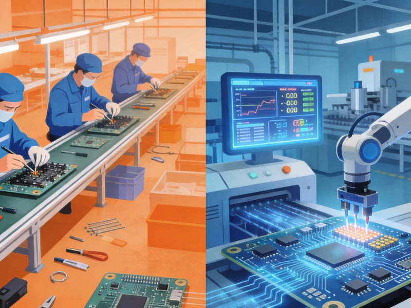
Comparing Traditional vs. Digital Quick Turn PCB ServicesJuly/18/2026
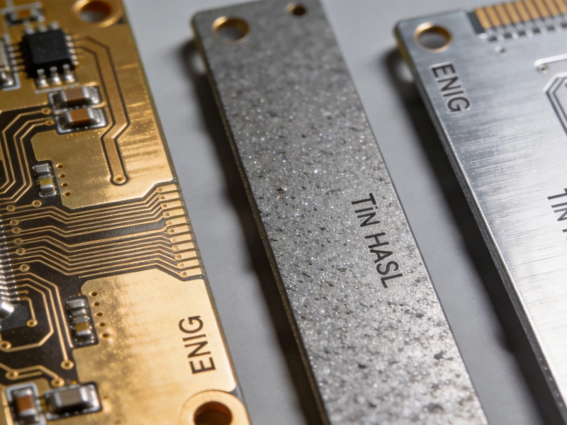
Custom Surface Finishes: Choosing Between ENIG, HASL, OSP, and Immersion SilverSeptember/14/2026
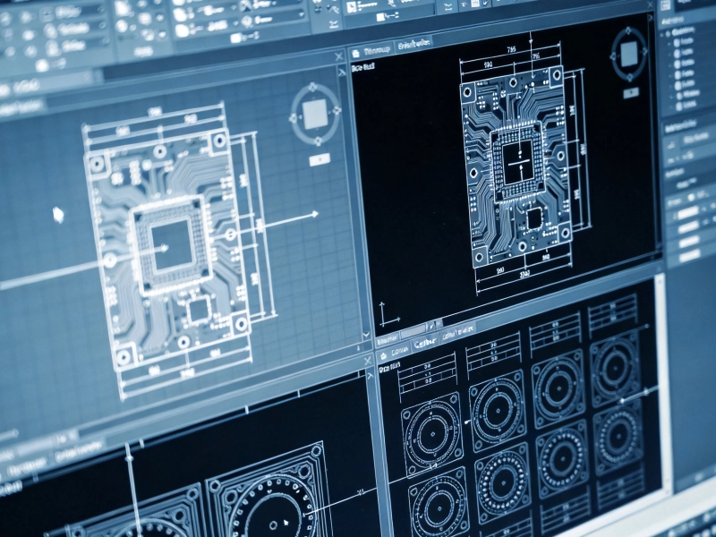
Best Practices for Preparing Files for Expedited PCB ManufacturingJuly/29/2026
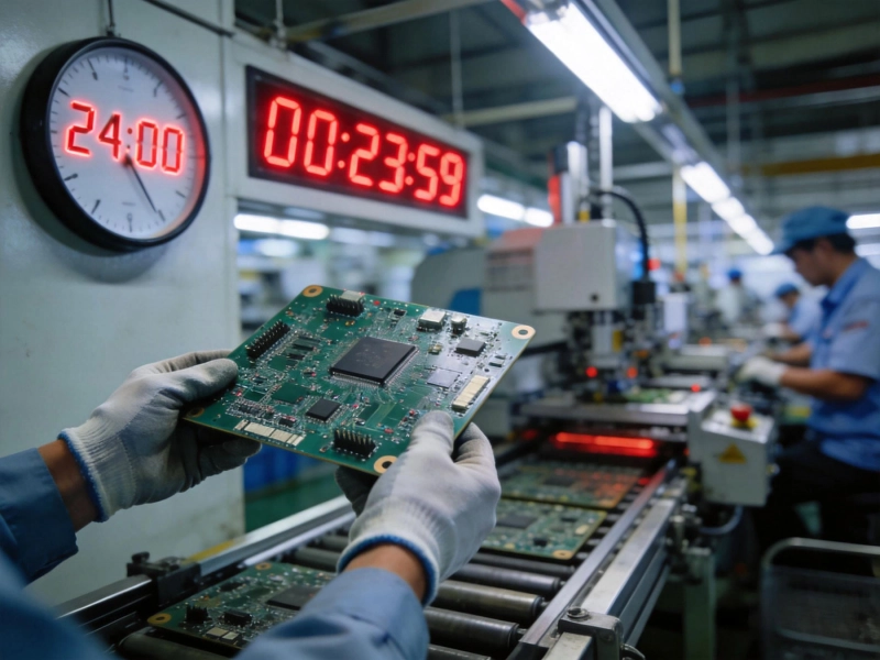
24-Hour Turnaround: Is it Possible and How Does it Work?May/21/2026
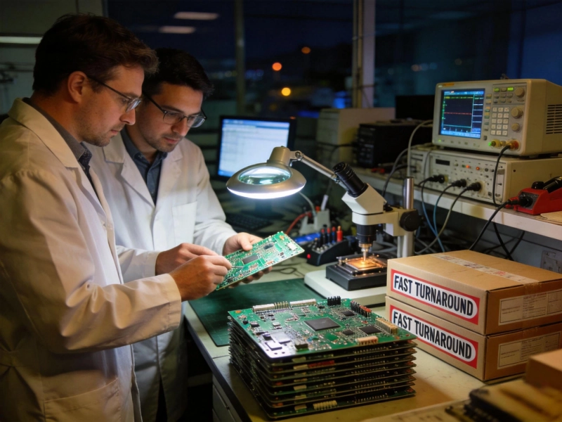
Why Quick Turn PCB Fabrication is Critical for R&D TeamsMay/21/2026

How AI-Driven Scheduling is Making Rapid PCB Prototyping More ReliableJune/18/2026
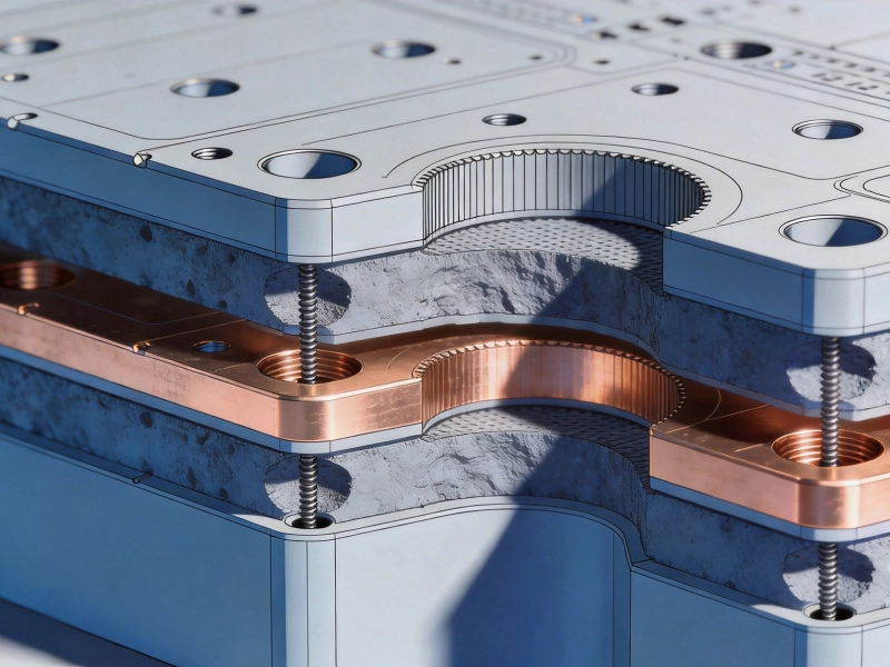
How to Specify Tolerances and Stack-ups for High-Precision Custom PCBsJuly/28/2026