
The landscape of Pcb Manufacturing has undergone significant transformation over the past decade. What once required weeks of lead time through traditional fabrication facilities can now be accomplished in hours through digital manufacturing technologies. Understanding the differences between traditional vs. digital Quick Turn Pcb services helps engineers, product teams, and hardware startups make informed decisions that balance speed, cost, and quality requirements.
Quick Turn services exist on a spectrum from fully traditional to fully digital, with hybrid approaches offering various combinations of speed, flexibility, and capability. This article examines the key distinctions, advantages, and limitations of each approach to help you select the optimal manufacturing path for your specific project needs.
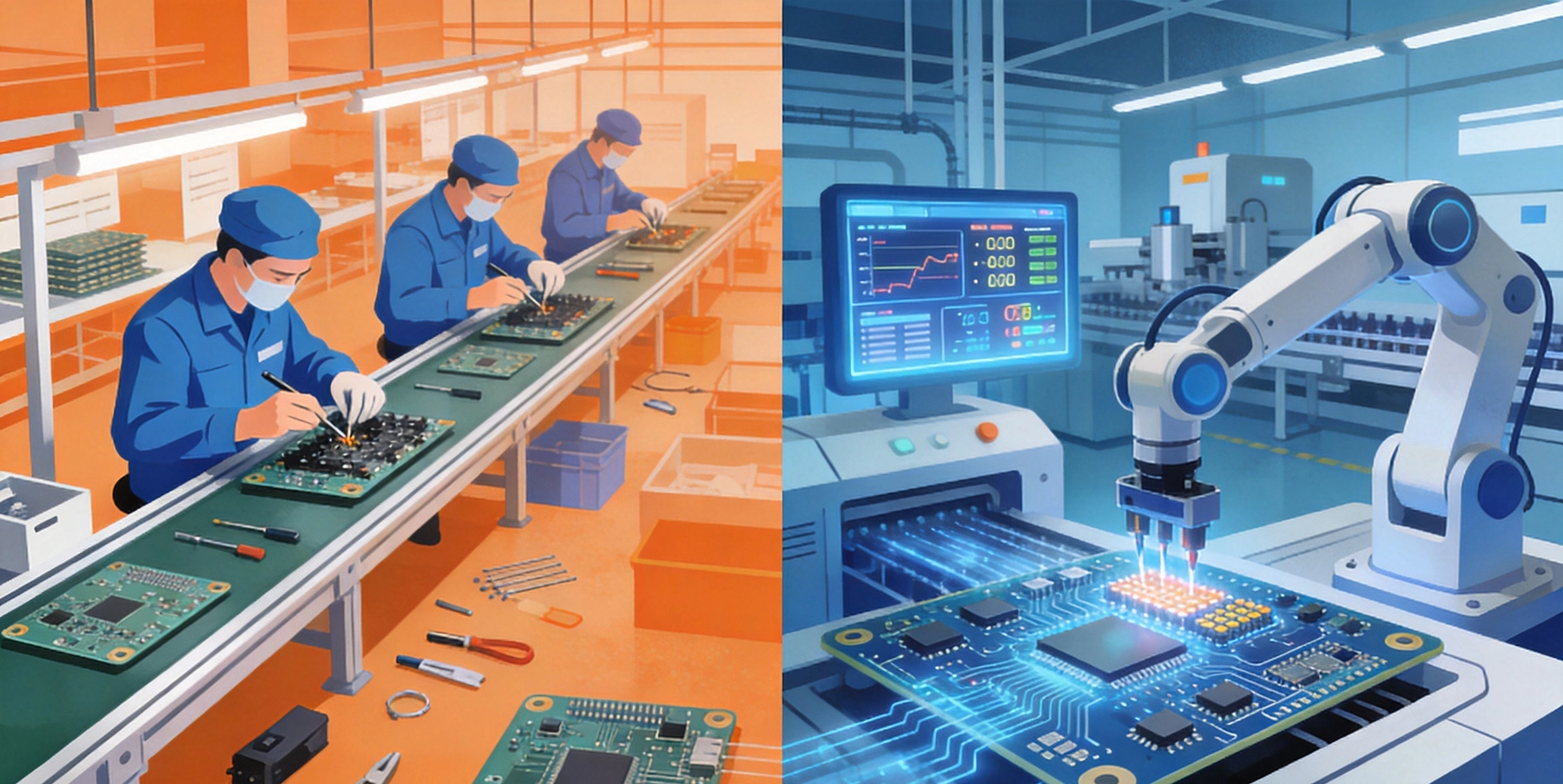
Traditional Pcb Manufacturing relies on subtractive processes that build circuits by removing copper from a fully clad substrate. The process begins with panel preparation—cutting substrate material to size—followed by drilling, copper plating, pattern application using Photolithography, chemical etching to remove unwanted copper, and surface finishing. Each step involves dedicated equipment, significant setup time, and careful process control.
Traditional facilities typically operate on batch processing models where multiple customer designs share production equipment. This batch approach optimizes equipment utilization but introduces queue times between steps. A typical traditional Quick Turn might offer 5-10 day delivery, while standard production runs commonly extend to 3-4 weeks or longer depending on facility capacity and order volume.
Traditional PCB Fabrication demands substantial capital investment in chemical processing lines, precision drilling equipment, and cleanroom facilities. A complete fabrication facility requires millions of dollars in equipment along with environmental controls for chemical waste management and air quality. These fixed costs drive minimum order requirements and influence pricing structures across the industry.
The equipment used in traditional manufacturing often represents decades of engineering refinement. Tunnel etching systems, automatic optical inspection stations, and sequential lamination equipment all contribute to high-quality output but require skilled operators and regular maintenance. This infrastructure creates significant barriers to entry, resulting in a relatively consolidated industry structure.
Traditional manufacturing excels at producing complex Multilayer Boards with advanced features including blind and Buried Vias, sequential lamination, Controlled Impedance, and specialized materials. These capabilities reflect decades of process development and remain essential for many demanding applications in aerospace, automotive, medical devices, and telecommunications.
However, traditional processes carry inherent limitations. Setup times for each production run create minimum economical batch sizes. The chemical processes involved introduce environmental variability that affects consistency. Design Rules must accommodate process tolerances accumulated across multiple steps. These factors combine to limit the flexibility available to customers ordering traditional PCBs.
Digital PCB manufacturing, often called additive or desk-top fabrication, fundamentally changes how circuits are created. Rather than removing copper through chemical etching, digital processes deposit conductive materials precisely where needed. This approach eliminates many setup steps, reduces material waste, and enables rapid transitions between different designs without reconfiguration.
Various digital technologies have emerged, including laser direct structuring (LDS), inkjet printing of conductive materials, and CNC milling with controlled depth penetration. Each technology offers distinct advantages and trade-offs in resolution, material options, and throughput. Laser-based approaches have gained particular traction for quick turn applications due to their precision and flexibility.
Digital manufacturing dramatically compresses the production timeline. Design files uploaded to a digital fabrication system proceed directly to production without the intermediate steps that characterize traditional manufacturing. No Photolithography masks, no chemical baths, no extended plating cycles—just direct digital fabrication from design data to finished board.
This streamlined workflow enables delivery times measured in hours rather than days or weeks. Some digital services offer same-day turnaround for simple designs, providing unprecedented responsiveness for Prototype development. The immediacy of digital manufacturing has proven particularly valuable for hardware startups iterating rapidly on early-stage designs.
Modern digital Pcb Services can produce functional boards with moderate complexity. Two-layer boards with standard Surface Mount components, through-hole parts, and basic routing represent the sweet spot for digital manufacturing. Line and space resolutions of 100-150 microns are achievable with current technology, enabling reasonably dense designs without sacrificing turn-around speed.
Multi-layer capability remains limited in the digital domain, though some systems can produce simple multilayer structures through sequential processing. The primary limitations involve material compatibility, via formation, and surface finish options compared to traditional processes. For advanced applications requiring six or more layers, blind/Buried Vias, or specialized laminates, traditional manufacturing typically remains necessary.
Traditional quick turn services typically promise delivery within 5-10 business days, with premium pricing for faster turnaround. Some facilities offer 24-hour or 48-hour expedited service at significant cost premiums. These timeframes reflect genuine manufacturing speed—once boards enter the production line, actual processing time may be relatively brief—but include substantial queue time during which orders wait for available equipment.
The speed of traditional manufacturing scales somewhat with order volume. A larger order requiring extended equipment runtime may actually receive priority treatment during scheduling, potentially delivering faster than a smaller quick turn order competing for the same equipment slots. Understanding your fabricator's scheduling logic helps set realistic delivery expectations.
Digital quick turn services routinely advertise same-day or next-day delivery, and these claims generally reflect actual capability rather than marketing hyperbole. The elimination of batch processing and chemical steps removes the primary sources of delay in traditional manufacturing. Small orders that would queue behind larger jobs in traditional facilities receive immediate processing in digital workflows.
Speed advantages extend beyond simple delivery time to include overall project cycle time. Immediate fabrication means engineers can iterate designs faster, receiving physical boards within hours of completing design modifications. This responsiveness compresses development timelines and enables more design iterations within fixed project schedules.
Rapid Prototyping benefits most dramatically from digital manufacturing speed. Hardware startups validating early concepts, engineers debugging board-level issues, and developers requiring functional boards for software development all benefit from digital quick turn immediacy. The ability to close the design-build-test loop within a single day enables an agile development approach that slower manufacturing prohibits.
Low-volume production of simple boards also favors digital services. When quantities required are small enough to be produced directly without batching, digital manufacturing eliminates the inefficiency of minimum order requirements. Educational institutions, hobbyists, and small research groups find particular value in services that can produce exactly the quantity needed without forcing purchases of unwanted additional boards.
Traditional PCB Fabrication operates under well-established quality frameworks including IPC industry standards and ISO certifications. The maturity of traditional processes means extensive documentation of failure modes, validated process controls, and trained quality personnel. Customers receive boards manufactured to recognized specifications with documented conformance to stated tolerances.
The chemical processes in traditional manufacturing, while introducing variability, also produce consistent results within well-defined process windows. Established fabricators understand their equipment capabilities and maintain processes within acceptable ranges. This consistency translates to predictable quality across multiple production runs from the same facility.
Digital Pcb Manufacturing Quality has improved substantially but varies more widely than traditional manufacturing. Service providers range from established companies with robust quality systems to smaller operations with limited process control. Understanding your digital manufacturer's quality practices becomes essential for ensuring reliable results.
Material properties in digital manufacturing may differ from traditional FR-4 substrates. Dielectric constants, thermal properties, and mechanical characteristics of digitally fabricated boards may not match datasheet specifications for standard materials. These differences rarely matter for Prototype validation but deserve consideration for designs targeting production deployment.
Quality requirements should drive manufacturing method selection. Functional prototypes for design validation can tolerate more variability than production-intent boards. Boards for demonstration units or limited field trials require intermediate quality levels. Only production deployments in demanding applications genuinely require the full Quality Assurance infrastructure of traditional manufacturing.
Matching manufacturing method to development stage makes economic sense. Rapid digital prototyping during development, transitioning to traditional manufacturing for production, leverages the advantages of each approach at the appropriate project phase. Some teams maintain parallel relationships with both traditional and digital suppliers to access this flexibility.
Traditional PCB pricing reflects the underlying cost structure of fabrication facilities: capital equipment depreciation, chemical consumption, labor for process monitoring, and facility overhead. These costs distribute across production volume, creating economies of scale that make traditional manufacturing increasingly economical as quantities increase. Traditional pricing typically shows significant per-board cost reduction as order quantity grows.
Setup costs represent a substantial component of traditional pricing regardless of order size. Engineering reviews, artwork preparation, tool setup, and first-article inspection occur for every order, creating a baseline cost that smaller orders cannot amortize effectively. This setup cost structure establishes minimum economical order sizes that may exceed actual requirements for some projects.
Digital Pcb Services typically employ simpler pricing structures with lower or no setup charges. Per-board pricing often remains relatively flat across small quantity ranges, reflecting the lower setup burden of digital manufacturing. This pricing model favors small orders that would pay disproportionate setup costs in traditional manufacturing contexts.
However, digital manufacturing does not benefit from the same economies of scale as traditional production. Per-board pricing may not decrease significantly with larger orders, limiting the cost advantage for moderate quantities. Understanding where traditional manufacturing becomes more economical based on quantity helps optimize procurement decisions.
Board cost represents only part of total project expense. Shipping, duties, inspection time, and the value of development cycle compression all factor into the true cost of PCB procurement. For time-sensitive projects, the premium pricing of digital quick turn services may represent excellent value compared to delays from traditional manufacturing scheduling.
Quality-related costs also affect total ownership. Boards requiring rework due to Fabrication Defects, delays from missed delivery commitments, and the engineering time spent managing supplier relationships all contribute to effective cost beyond quoted prices. These factors favor reliable suppliers regardless of their manufacturing approach.
Traditional Pcb Design incorporates process constraints from the manufacturing facility. Minimum line width, spacing, and annular ring dimensions reflect fabrication tolerances. Via sizes and aspect ratios limit routing density. Surface finish options depend on available processes. These constraints are well-documented and accommodated by standard EDA software design rule checking.
Working closely with your fabricator during design improves outcomes. Most traditional manufacturers provide design guidelines specifying their actual capabilities, which may differ from theoretical limits. Early engagement identifies potential issues before manufacturing, preventing costly revisions or delays when designs fail process requirements.
Digital manufacturing imposes different design constraints than traditional processes. Trace geometry may be limited by deposition or milling resolution. Via formation differs from drilled-through holes. Material selection reflects available substrates. These differences require adaptation of design approaches to digital capabilities.
Some designs require modification to work effectively with digital manufacturing. High-density routing may need relaxation. Layer counts may need reduction. Component packages may need substitution. Understanding digital manufacturing constraints during schematic and layout design prevents surprises when boards return from fabrication.
Many organizations employ hybrid manufacturing strategies that leverage both traditional and digital services depending on project requirements. Early prototypes and design iterations typically favor digital speed. Pre-production validation and first articles may use traditional manufacturing for representative samples. Production deployment returns to traditional manufacturing for cost-effective high-volume output.
Building relationships with multiple suppliers across both categories provides flexibility and negotiating leverage. Understanding each supplier's strengths and limitations enables intelligent routing of designs to appropriate facilities. This supplier diversity also provides risk mitigation—Supply Chain disruptions affecting one supplier can be addressed through alternative sources.
Choosing between traditional and digital Quick Turn Pcb services requires understanding your project's specific priorities across speed, cost, quality, and capability dimensions. Traditional manufacturing offers superior capability for complex multilayer designs and becomes cost-effective at higher volumes, while digital manufacturing provides unmatched speed and flexibility for simple to moderately complex designs in small quantities.
The most effective approach often combines both methods strategically: using digital services for Rapid Prototyping during development, then transitioning to traditional manufacturing for production deployment. This hybrid strategy maximizes the advantages of each while minimizing their respective limitations.
As digital manufacturing technology continues advancing, the boundary of what's possible with quick turn services will continue expanding. Staying current with supplier capabilities and industry developments ensures access to the most effective manufacturing options as your project needs evolve.
Microvias and Blind/Buried Vias: Key Technologies in HDI FabricationAugust/11/2026

Emergency PCB Runs: Strategies for Getting Boards Fast Without Sacrificing ReliabilityJuly/08/2026
Understanding the Basics of PCB Production China: From Gerber Files to Finished BoardsOctober/16/2026
Thermal Management Strategies for Dense Multilayer PCB DesignsJuly/31/2026
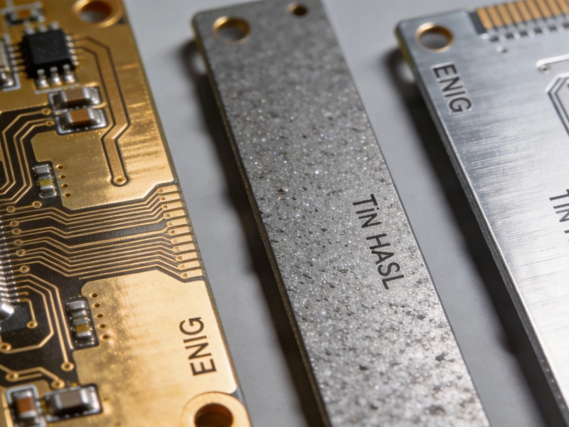
Custom Surface Finishes: Choosing Between ENIG, HASL, OSP, and Immersion SilverSeptember/14/2026
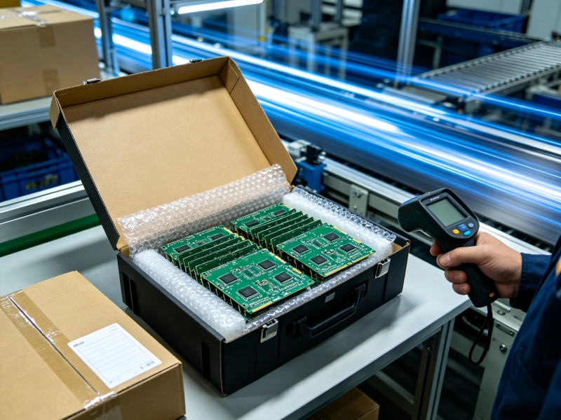
The Logistics of Speed: Shipping and Handling for Urgent PCB DeliveriesSeptember/03/2026
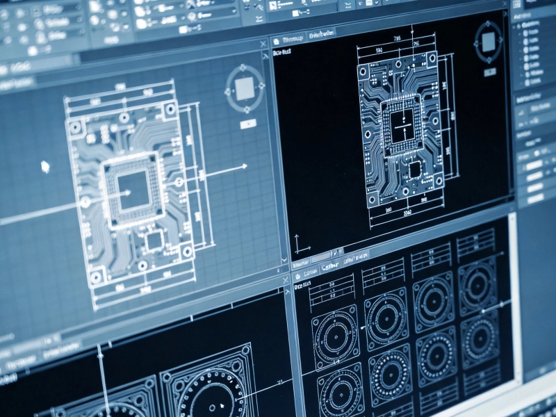
Best Practices for Preparing Files for Expedited PCB ManufacturingJuly/29/2026
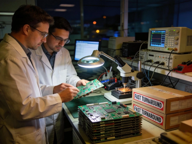
Why Quick Turn PCB Fabrication is Critical for R&D TeamsMay/21/2026