
Copper is the lifeblood of every printed circuit board. Without copper conductive traces carrying signals and power between components, a PCB would be nothing more than an inert piece of fiberglass. But copper on a raw board is only the starting point. What transforms a bare laminate into a functional circuit is copper plating—a precisely controlled electrochemical process that builds up copper layers inside drilled holes, on surface traces, and at solder pads to create reliable electrical connections that last for years.
Understanding copper plating is essential for anyone involved in Pcb Design, procurement, or Quality Assurance. The strength and reliability of every electrical connection on your board depends directly on the quality of the copper plating process. In this article, we will explain how copper plating works, why it matters so much for PCB performance, the different plating methods used in manufacturing, and what you should look for when evaluating a Pcb Supplier's plating capabilities.
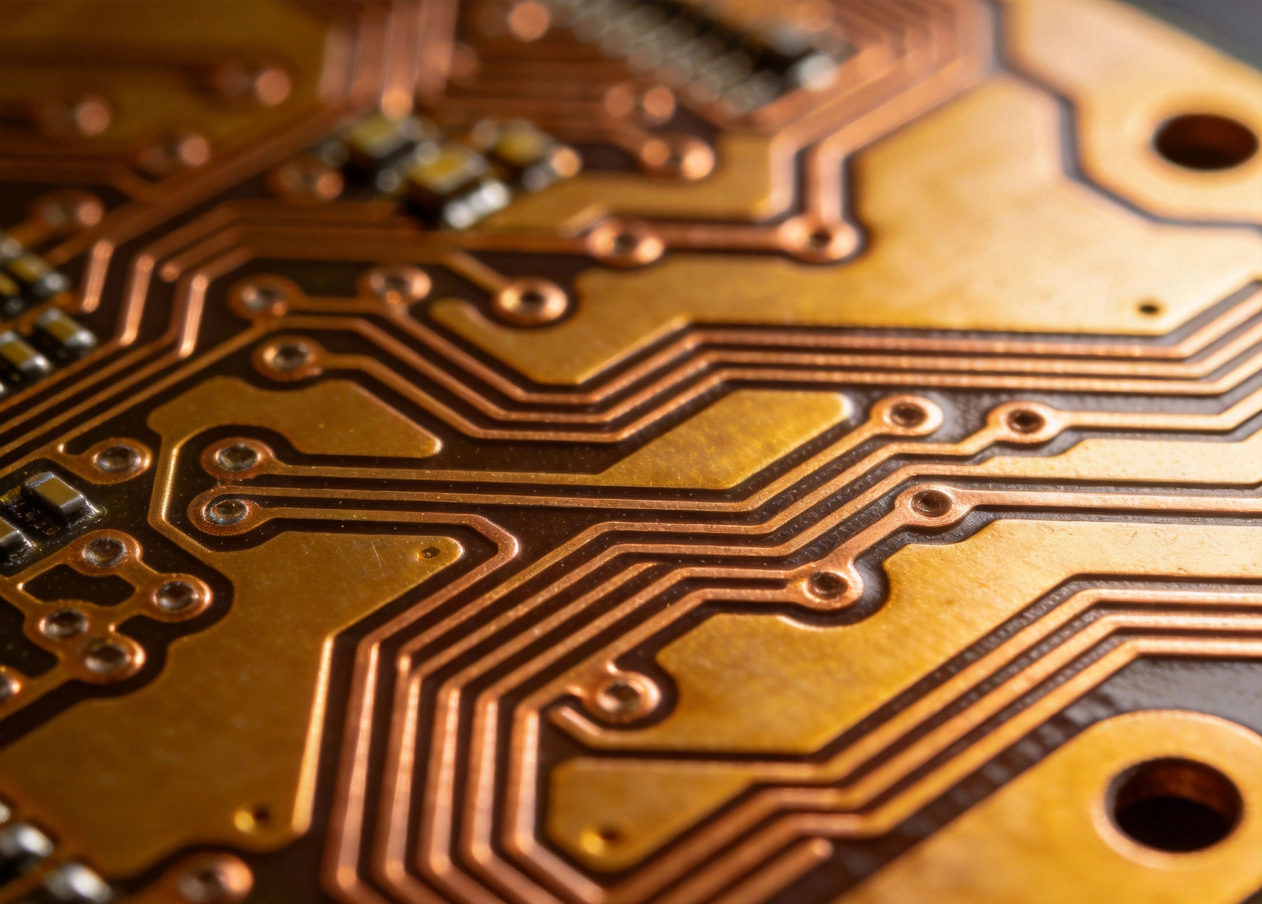
Copper plating serves multiple purposes on a PCB, and each one has direct consequences for how your board performs in the field.
The most obvious function is creating conductive traces. When you route copper on your Pcb Layout, you are designing the pathways along which electrons will travel. But copper traces alone are only half the story. The moment you drill a hole through your board to connect one layer to another, you need a conductive bridge inside that hole. Copper plating fills that hole with metal, creating what is called a plated through-hole (PTH) or via. Without proper copper plating inside those holes, there is no electrical connection between layers, and your Multilayer Board would not function at all.
Beyond connectivity, copper plating also determines the mechanical durability of your board. The copper barrel inside each plated through-hole must withstand the thermal stress of soldering, the vibration of real-world use, and the repeated thermal cycling that occurs every time the device powers on and off. Poorly plated holes crack under this stress, leading to intermittent failures that are notoriously difficult to diagnose. High-quality copper plating gives your board the durability to survive years of operation in demanding environments.
Additionally, the thickness of the copper plating directly affects current-carrying capacity. Thicker copper can handle more current without overheating, which is why high-power applications require boards with heavier copper weights. When designing Power Electronics, choosing the right copper thickness is not just a performance decision—it is a safety decision.
PCB copper plating is an electrochemical process, which means it uses an electrical current to deposit copper metal from a solution onto the surface of the board. The board is immersed in an electrolyte solution containing dissolved copper salts, typically copper sulfate, along with sulfuric acid and various proprietary additives that control the properties of the deposited metal.
The board acts as the cathode, meaning it carries a negative electrical charge. A set of copper anodes, which are bars of pure copper, carry a positive charge and sit on the opposite side of the plating tank. When electrical current flows through the solution, copper atoms from the anodes dissolve into the electrolyte and are simultaneously attracted to and deposited onto the surface of the board. This process is called electroplating, and it is the workhorse of PCB copper deposition.
For through-hole plating, the process is more involved. Before copper can be deposited inside the holes, the board must first be sensitized with a thin layer of palladium catalyst, which allows the non-conductive hole walls to accept an initial thin copper coating through a process called electroless copper plating. Electroless plating is a chemical reduction process that does not require electrical current, and its sole purpose is to make the inside of the drilled holes conductive enough to accept the subsequent electroplating step. Once a thin conductive base layer exists, the board moves to the electroplating tank where the full copper thickness is built up to specification.
Panel plating is the most common and straightforward plating method. In panel plating, the entire surface of the board—including the areas that will become traces and the large open areas between them—is plated with copper. After plating, the unwanted copper is etched away, leaving only the designed trace pattern. This approach is efficient and works well for most standard PCB designs. The uniformity of plating thickness across the board is relatively consistent, making it predictable and reliable for most applications.
Pattern plating takes a different approach. Instead of plating the entire surface, only the areas that will become traces and pads are selectively plated. The board is covered with a plating resist that protects the non-trace areas during the plating process. After copper is deposited in the desired pattern, the resist is stripped and the board is etched to remove any thin layer of copper that may have been deposited on the non-resist areas. Pattern plating offers tighter control over trace geometry and is often preferred for fine-line designs where trace width and spacing tolerances are critical. It is more expensive than panel plating due to the additional process steps but delivers superior results for high-density designs.
Backlight plating is a hybrid technique used for high-reliability applications. In this process, the board is first pattern plated to define the traces. Then, a thin layer of additional copper is applied uniformly across the entire board surface, including over the traces. This extra copper builds up the cross-sectional area of the traces, improving current-carrying capacity and thermal performance. Backlight plating is commonly specified for aerospace, automotive, and high-power applications where Board Reliability is non-negotiable.
When discussing copper plating on PCBs, you will encounter two related but distinct terms: copper thickness and copper weight. They are closely related because one is a direct physical measurement and the other is a practical industry convention.
Copper weight, expressed in ounces per square foot (oz/ft²), refers to the weight of copper that would cover one square foot of board surface to a depth of one mil, which is 0.001 inch or approximately 1 mil. Standard PCB copper weight is 1 oz/ft², which corresponds to approximately 1.37 mils or 34.8 micrometers of thickness. Other common weights include 0.5 oz/ft² (half-ounce, about 0.7 mils), 2 oz/ft² (about 2.8 mils), and heavier weights like 3 oz/ft² and 4 oz/ft² for high-power applications.
The actual copper thickness after plating can vary slightly from the nominal weight due to process variations. Ipc Standards specify minimum and maximum acceptable thickness ranges, and reputable manufacturers maintain tight control over this parameter. When you specify a copper weight on your fabrication drawing, you should also specify whether you need the minimum or the nominal thickness, as this affects how the manufacturer sets up their plating process.
Not all copper plating is created equal. Several specific quality parameters determine whether a plated board will perform reliably in your application.
Void-free plating means that the copper fills the drilled holes completely without any air pockets, gaps, or voids. Even a small void in a plated through-hole creates a point of mechanical weakness where the copper barrel can crack under thermal stress. Achieving void-free plating requires rigorous process control, proper hole preparation, and adequate plating time. Manufacturers use cross-sectional analysis of sample boards to verify void-free quality, and Ipc Standards define maximum acceptable void sizes for different reliability classes.
Copper ductility refers to how much the plated copper can bend and flex without cracking. Highly stressed plating, often caused by high current density during electroplating or inappropriate additive concentrations, produces brittle copper that cracks under thermal cycling. High-quality Pcb Plating produces ductile copper with elongation of 15 to 20 percent or more, which allows the barrel inside the hole to flex slightly as the board expands and contracts during temperature changes. You can evaluate plating ductility through micro-sectioning and microscopy analysis of test coupons from each production lot.
Throwing power describes how evenly the plating solution deposits copper across different surface geometries. A solution with good throwing power ensures that inside-hole copper thickness is as close as possible to the surface copper thickness. Poor throwing power produces thinner copper in holes and on recessed surfaces compared to raised areas, which is undesirable because hole barrels are already the most mechanically stressed part of a plated board. Quality plating processes use additives that improve throwing power and ensure consistent coverage throughout the board, even on complex multilayer constructions.
Plated copper must survive multiple thermal cycles without degradation. The industry standard thermal stress test involves floating the board in molten solder at 288 degrees Celsius for 10 seconds and then examining the plated through-holes under magnification for cracks or delamination. IPC Class 2 and Class 3 boards have different acceptance criteria for this test, with Class 3 being more stringent. For mission-critical applications in automotive, aerospace, or medical electronics, boards should meet Class 3 thermal stress requirements to ensure they can withstand the thermal demands of their operating environment.
Even with rigorous process control, defects can occur during copper plating. Understanding these defects and how they affect your board will help you make better sourcing decisions and interpret quality reports from your manufacturer.
Copper voids and cracks are perhaps the most serious defects, as they compromise the structural integrity of plated through-holes and can cause field failures that are difficult to trace. These defects are best detected through microsectioning, where a small sample of the board is cut, mounted in epoxy, polished to a mirror finish, and examined under a microscope at high magnification. Flying Probe Electrical Testing can also detect open circuits caused by voids, but it cannot pinpoint the location of the defect.
Under-plating occurs when the copper thickness inside holes falls below the specified minimum. This is typically caused by insufficient plating time, poor throwing power in the electrolyte, or inadequate surface preparation. Under-plated holes have reduced current-carrying capacity and are more susceptible to failure from electromigration and thermal stress. Dimensional verification through microsectioning is the most reliable way to confirm copper thickness on hole walls.
Epitaxial copper separation is a more subtle defect where the copper layer separates from the base material at the copper-substrate interface. This can occur when the board surface is contaminated or insufficiently cleaned before plating. The separation creates a gap that acts as a mechanical weakness point, and the plated copper can delaminate under stress. This defect is often visible in cross-sections and requires a thorough review of the manufacturer's pre-plating cleaning process.
Surface roughness is a less critical but still noteworthy defect. Excessive roughness on plated copper traces increases surface area and can affect Impedance Control in high-frequency designs. While it does not necessarily cause functional failure, roughness can interfere with fine-pitch component placement and Solderability. Surface roughness is typically measured in micro-inches and can be checked with profilometry instruments.
While the manufacturing process plays the largest role in plating quality, your Pcb Design decisions also have a significant impact. Following good design practices reduces the risk of plating defects and improves the overall reliability of your board.
After copper plating is complete, the board receives a surface finish that protects the underlying copper from oxidation and provides a solderable surface for component assembly. Different surface finishes have different requirements for the underlying copper quality and affect the board in different ways.
Enig (Electroless Nickel Immersion Gold) is one of the most common surface finishes and requires high-quality copper plating as a foundation because the nickel layer is deposited directly onto the copper. Any surface roughness or contamination on the copper will be magnified by the Enig process. Hasl (Hot Air Solder Leveling) is more forgiving of surface irregularities because the hot solder reflow process smooths out minor surface variations. Osp (Organic Solderability Preservative) is the most sensitive to surface quality because the thin organic coating relies on a pristine copper surface for proper adhesion.
When specifying a surface finish, consider the assembly requirements and the base copper quality as a package. High-reliability boards with ENIG finish should always be evaluated for base copper quality through microsectioning, especially if the boards will undergo multiple thermal cycles in service.
The most common standard copper weight for general-purpose PCBs is 1 oz/ft², which equals approximately 1.37 mils (34.8 micrometers) of copper thickness after plating. For higher current applications, 2 oz/ft² (about 2.8 mils) or 3 oz/ft² (about 4.1 mils) copper weights are used. Specialty applications may require heavier copper weights of 4 oz/ft² or more.
Copper plating thickness is measured using several methods. X-ray fluorescence (XRF) is the most common non-destructive method, using X-rays to determine the elemental composition and thickness of the copper layer. For through-hole copper, microsectioning provides the most accurate measurement by physically cross-sectioning a sample board and examining it under a microscope. Eddy current testing is another non-destructive method used for surface copper thickness measurement.
Voids in plated through-holes are caused by trapped air or gas bubbles inside the hole during the plating process, inadequate surface preparation that prevents copper from adhering properly, insufficient plating solution flow into the hole, or plating process parameters that are not optimized for the hole aspect ratio. Ensuring proper hole cleaning, using adequate agitation in the plating tank, and controlling the plating current density appropriately all help minimize voids.
Yes, copper plating can affect Signal Integrity in high-frequency designs. The roughness of the plated copper surface impacts the skin effect at high frequencies, causing signal attenuation. Additives used in the plating process can influence grain structure and surface roughness. For microwave and RF applications operating above several gigahertz, specifying low-roughness copper plating or alternative deposition methods may be necessary to achieve the required signal performance.
Your fabrication drawing should specify the minimum copper weight for outer layers and inner layers separately, any base copper weight before plating if using a specific base copper foil, the minimum acceptable hole wall copper thickness (typically 0.7 mil to 1.0 mil depending on reliability class), the surface finish specification, and any reliability class requirements such as IPC Class 2 or Class 3. The more specific you are, the better your manufacturer can meet your requirements.
Copper plating is far more than a manufacturing step—it is the foundation of every PCB's electrical and mechanical performance. The quality of copper inside your plated through-holes, the uniformity of your traces, and the durability of your board under thermal and mechanical stress all depend on how well the plating process is controlled. By understanding the fundamentals of copper plating, the different methods available, the key quality parameters to watch, and how your design decisions influence plating outcomes, you become a better partner to your manufacturing supplier and a more effective designer.
When you specify copper plating requirements clearly, demand appropriate quality verification from your supplier, and follow good design practices, you set the stage for reliable boards that perform consistently from the first power-on to years of field operation. Whether you are building consumer electronics or mission-critical automotive systems, the principles of quality copper plating remain the same: void-free coverage, ductile material, controlled thickness, and rigorous verification.
This article is provided for general informational purposes regarding PCB copper plating processes and quality standards. Specific Manufacturing Capabilities and specifications may vary by supplier and application requirements.
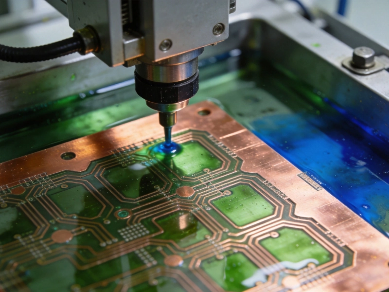
Etching Explained: How Circuit Patterns are Precisely Formed on Copper Clad LaminatesJuly/30/2026
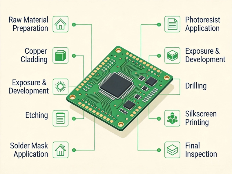
A Step-by-Step Walkthrough of the PCB Fabrication ProcessMay/21/2026

E-Commerce vs. Traditional Sales: How Buying PCB Services Has ChangedJuly/25/2026

How Automation is Revolutionizing China's PCB SectorJune/03/2026
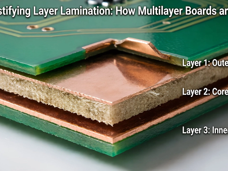
Demystifying Layer Lamination: How Multilayer Boards are BuiltJune/05/2026
Is PCB Fabrication in China Still the Most Cost-Effective Option? A 2026 AnalysisJuly/27/2026
Visualizing the Flow: An Infographic Guide to How Your PCB is MadeSeptember/24/2026

The Chemistry of PCB Cleaning: Why Ionic Contamination MattersSeptember/04/2026