Open Nav

The relentless march of Electronics Miniaturization has pushed printed circuit board technology to extraordinary heights. As devices become smaller, more powerful, and more complex, Traditional Pcb technologies face fundamental limitations in component density and interconnect capabilities. Any-layer interconnect technology represents the cutting edge of high-density interconnect (HDI) Pcb Design, enabling unprecedented levels of component integration and electrical performance. This advanced technology, once the exclusive domain of aerospace and military applications, has matured into commercially viable solutions for consumer electronics, automotive systems, and telecommunications infrastructure. Understanding any-layer interconnect technology is essential for engineers seeking to design the next generation of compact, high-performance electronic products.
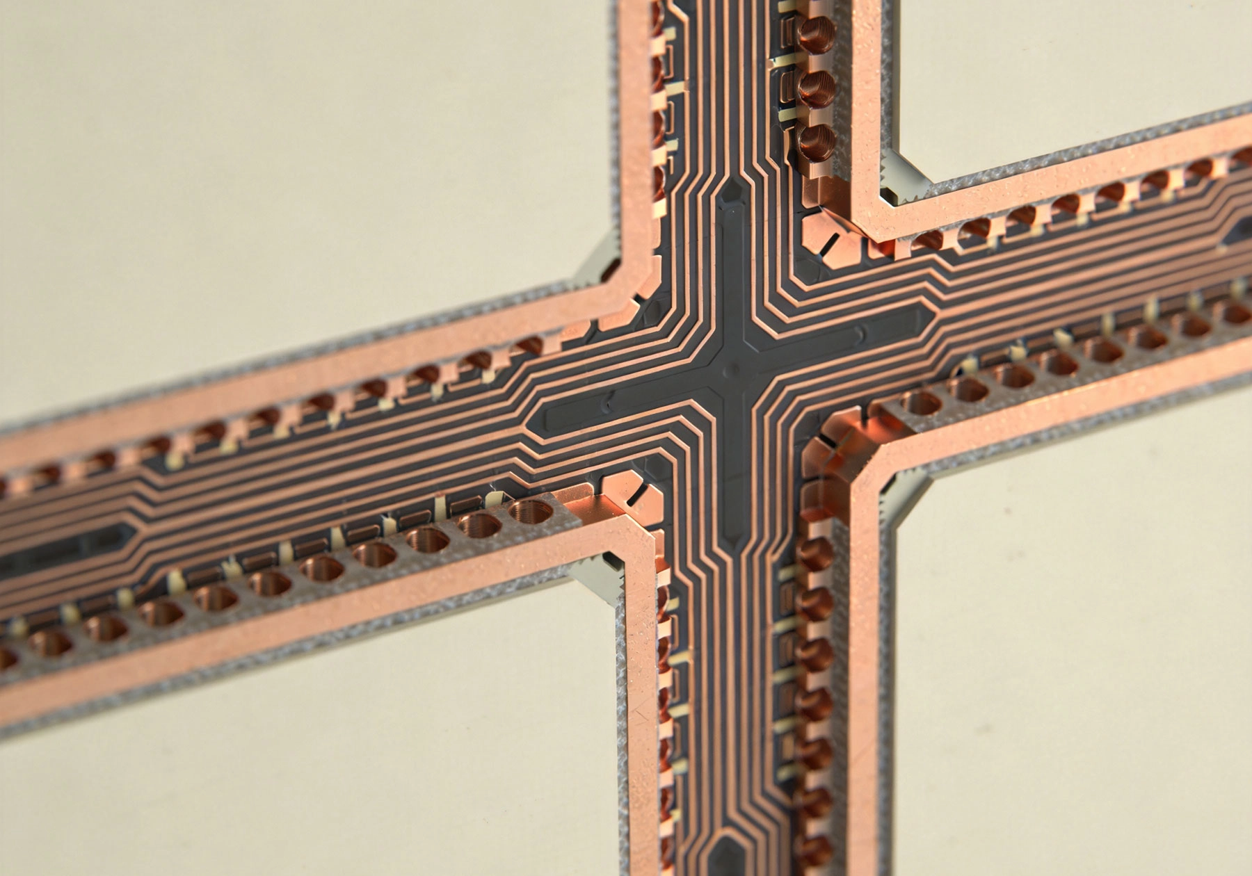
Before diving into any-layer interconnect specifics, it's crucial to understand the broader context of HDI technology. HDI PCBs emerged in response to the need for greater component density, finer pitch requirements, and improved Signal Integrity in modern electronic devices.
Traditional Pcb technology relied primarily on through-hole vias and plated through holes (PTHs) to create electrical connections between copper layers. While effective for many applications, PTHs consume significant board area and impose constraints on trace routing density. As component packages became smaller and pin counts increased, the limitations of traditional through-hole technology became increasingly apparent.
The transition to Surface Mount Technology (SMT) enabled smaller components but created new challenges for interconnection density. Ball grid arrays (BGAs), chip-scale packages (CSPs), and other high-pin-count devices required smaller vias positioned closer together than traditional manufacturing processes could support. HDI technology emerged to address these challenges through Microvias, finer trace widths, and more sophisticated layer stacking.
HDI design fundamentally changes how engineers approach Pcb Layout. Instead of treating layers as simple copper planes connected by large through-hole vias, HDI treats the PCB as a three-dimensional interconnect structure. Multiple thin dielectric layers, Microvias with diameters as small as 50 micrometers, and stacked via structures enable routing density that would be impossible with traditional approaches.
The philosophy shifts from maximizing board area efficiency to optimizing three-dimensional routing through multiple layers. This approach enables functionality that would require larger boards or multiple boards in traditional designs to be consolidated into a compact, highly integrated single board.
HDI encompasses several enabling technologies that work together to achieve high interconnect density:
Any-layer interconnect represents the ultimate expression of these technologies, pushing HDI capabilities to their theoretical limits.
Any-layer interconnect technology enables electrical connections between any two layers of a multi-layer PCB, regardless of their position in the layer stack. This capability fundamentally changes how designers approach routing and interconnect architecture.
The core enabling technology for any-layer interconnect is the Microvia. Unlike traditional mechanically drilled through-hole vias that penetrate the entire board thickness, microvias are small, laser-drilled holes that typically span only one or two dielectric layers.
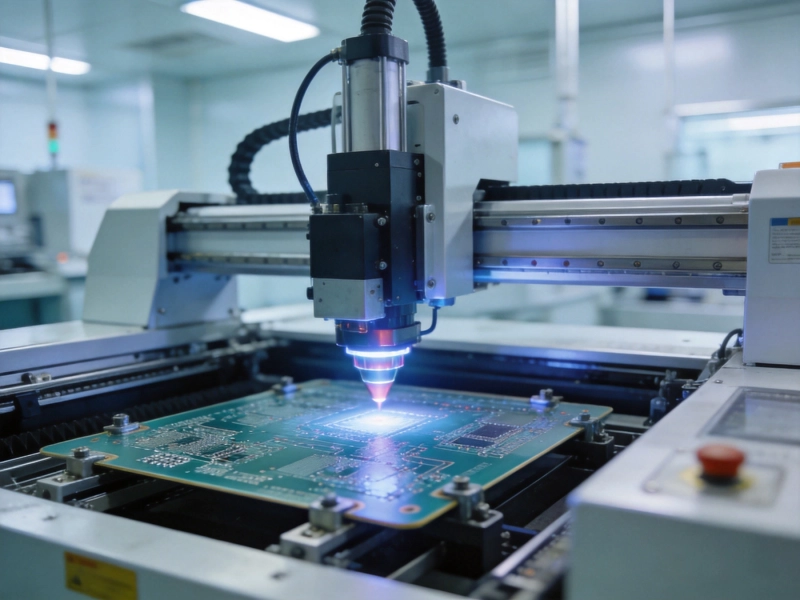
Laser drilling systems, particularly UV laser systems, can create microvias with diameters as small as 50 micrometers (approximately 2 mils). This precision enables via placement within component pads and extremely dense via arrays. The small diameter also reduces parasitic inductance and capacitance, improving Signal Integrity for high-speed designs.
Microvias can be of several types:
The true power of any-layer interconnect lies in stacked via structures. By precisely aligning microvias on multiple layers, electrical connections can be established between any two layers in the stack. This capability requires exceptional manufacturing precision and process control.
Stacked vias create vertical interconnects that can span the entire board thickness without consuming large areas on each layer. This enables routing density that is simply impossible with traditional through-hole vias. For example, a connection between layers 2 and 8 in a 10-layer board would traditionally require a through-hole via occupying space on all 10 layers. With stacked microvias, the connection uses space only on the layers actually traversed, freeing up routing space on intervening layers.
Creating any-layer interconnect structures requires a sequential lamination process. Rather than laminating all layers together in a single operation, the board is built layer by layer, with microvias created and plated between lamination steps.
Typical process steps include:
This sequential approach enables microvias to be placed on any layer, not just outer layers, and allows stacked via structures to be built incrementally. The process requires careful control of dielectric thickness, via filling, and plating quality to ensure reliable interconnects.
Microvias in any-layer interconnect structures are typically filled with conductive material rather than left as empty holes. This filling serves multiple purposes: it provides a flat surface for subsequent processing, prevents solder wicking during assembly, and improves reliability under thermal cycling.
Copper filling is the most common approach, though conductive epoxy and other materials are sometimes used. Filled vias provide better thermal conductivity than empty vias and can serve as thermal paths for heat dissipation from components.
Any-layer interconnect technology delivers several key performance advantages that make it indispensable for advanced electronic products.
The most obvious advantage of any-layer interconnect is the dramatic increase in routing density. By enabling connections between any two layers without occupying space on intervening layers, designers can place components and traces much more densely than with traditional PCB technology.
Density improvements of 200-300% over conventional HDI and 500% or more over through-hole technology are achievable. This density enables functionality that previously required multiple boards or larger form factors to be implemented in compact single boards.
The space savings from reduced via size and stacked via structures are compounded by the ability to use finer trace widths and smaller clearances. Modern any-layer designs routinely use 2-3 mil traces and spaces, with some advanced capabilities reaching 1-2 mil.
Any-layer interconnect improves signal integrity through multiple mechanisms. Smaller via diameters reduce parasitic inductance and capacitance, which is particularly important for high-speed signals. Stacked vias provide shorter electrical paths than equivalent through-hole vias, reducing signal delays.
The ability to place microvias within component pads enables more direct routing with fewer discontinuities. This is especially beneficial for BGAs and other high-density packages where conventional routing would require long detours through multiple vias.
Controlled Impedance routing becomes easier with the increased routing options available in any-layer designs. Designers can more easily achieve target impedance values while maintaining signal integrity requirements.
Thermal Management is a growing concern in compact electronic designs, and any-layer interconnect contributes several thermal advantages. Filled microvias provide thermal paths between layers, enabling heat from components on outer layers to spread into inner copper planes.
The higher copper density achievable with any-layer designs improves overall thermal conductivity of the PCB. More copper area provides more thermal mass and more surface area for heat dissipation.
Designers can strategically place thermal microvias under high-power components to conduct heat into internal copper planes or to the opposite side of the board where heat sinks or cooling solutions can be more effectively applied.
Power distribution networks benefit from the increased routing density and copper area available in any-layer designs. Power and ground planes can be placed on multiple layers, providing low-resistance paths throughout the board. Decoupling capacitors can be placed closer to IC power pins with short, low-inductance connections via microvias.
The ability to connect any layer to power or ground planes via microvias enables more robust power distribution with better voltage regulation and reduced noise. This is particularly important for high-current applications and designs with mixed signal requirements.
Any-layer interconnect technology has found applications across diverse industries where miniaturization and performance are critical.
Smartphones, tablets, and wearable devices represent some of the largest applications for any-layer interconnect technology. The relentless demand for smaller, more powerful devices drives adoption of the most advanced PCB technologies available.
In smartphones, any-layer interconnect enables integration of processor, memory, camera, wireless connectivity, and power management functions into a board area that might be only 20-30 square centimeters. The complexity approaches that of full-sized computers in a fraction of the space.
Wearables present even more stringent requirements. Smartwatches and fitness trackers must integrate sophisticated functionality into boards only a few centimeters square, often with non-rectangular shapes to fit device ergonomics. Any-layer interconnect makes these designs possible.
Laptops, ultrabooks, and 2-in-1 devices leverage any-layer interconnect for both main boards and smaller peripheral boards. The trend toward thinner, lighter devices with increased performance drives adoption of high-density interconnect technologies.
Processor and power management subsystems benefit from the improved power distribution and Thermal Management capabilities of any-layer designs. High-speed memory interfaces require the signal integrity improvements that microvias provide.
Modern vehicles incorporate dozens of electronic control units (ECUs) for functions ranging from engine management to infotainment. Space constraints and reliability requirements make any-layer interconnect attractive for automotive applications.
Advanced driver assistance systems (ADAS) with multiple cameras, radar, and lidar sensors require high-density processing boards that leverage any-layer capabilities. The automotive temperature range and vibration environment demand robust interconnect structures that can withstand harsh conditions.
5G telecommunications equipment operates at higher frequencies with greater bandwidth than previous generations. High-frequency signals require exceptional signal integrity and electromagnetic compatibility, which any-layer interconnect supports through reduced parasitics and optimized routing.
Network switches, routers, and base station equipment incorporate any-layer interconnect for both digital processing boards and RF front-end modules. The combination of high pin count, high frequency, and space constraints makes any-layer technology essential.
Aerospace applications pioneered many HDI technologies and continue to push the boundaries of what's possible. Avionics, satellite electronics, and missile systems require extreme reliability in challenging environments with space at a premium.
High-performance computing modules for radar, sonar, and electronic warfare systems leverage any-layer interconnect for both digital processing and high-speed analog interfaces. The military's performance requirements and environmental constraints justify the premium cost of advanced HDI technology.
While any-layer interconnect delivers impressive capabilities, it also presents significant manufacturing challenges that affect cost, yield, and Design Rules.
Manufacturing any-layer interconnect boards requires substantial investment in specialized equipment and process expertise. UV laser drilling systems with precision positioning and power control are essential for reliable microvia creation. Sequential lamination equipment with tight process control enables consistent layer-to-layer registration.
Plating processes must be optimized for microvia filling and reliable through-hole plating on complex structures. Quality Control equipment including automated optical inspection (Aoi), X-ray Inspection, and Electrical Testing must be capable of detecting defects in dense, complex structures.
The specialized nature of this manufacturing means that not all PCB fabricators can produce any-layer interconnect boards. Selecting capable suppliers requires careful evaluation of equipment, processes, and experience.
Any-layer interconnect imposes design constraints that differ from conventional Pcb Design:
Designers must balance these constraints against the benefits of any-layer interconnect. Trade-offs between density, cost, and manufacturability require careful consideration throughout the design process.
Any-layer interconnect boards command significant cost premiums over conventional PCBs. Multiple factors contribute to this cost:
Despite these costs, any-layer interconnect can be cost-effective when it enables functionality that would otherwise require multiple boards or larger devices. The total system cost must be evaluated, not just the PCB cost alone.
Reliability is paramount in high-value applications that use any-layer interconnect. The complex structure of stacked microvias presents potential failure modes that must be managed:
Rigorous testing including thermal cycling, drop testing, and Accelerated Life Testing is essential to ensure reliability requirements are met. Design techniques such as using staggered vias where possible, maintaining adequate aspect ratios, and ensuring robust plating quality help maximize reliability.
Successful any-layer interconnect design requires adherence to established guidelines and best practices that balance capability with manufacturability.
Microvia design requires careful attention to several parameters:
The layer stack configuration significantly affects manufacturability and performance:
Take full advantage of any-layer interconnect capabilities:
Incorporate thermal considerations into the design:
The field of high-density interconnect continues to evolve, with new technologies pushing the boundaries of what's possible.
Embedding passive components and even active ICs within the PCB layers represents the next evolution of high-density integration. This approach reduces board area further by eliminating Surface Mount components and reducing interconnect lengths.
Any-layer interconnect enables dense routing to and from embedded components, supporting increasingly complex embedded subsystems. Capacitors, resistors, and even simple ICs can be embedded during the lamination process.
The integration of system-in-package (SiP) and 3D packaging technologies with advanced PCBs creates even higher levels of integration. Multi-chip modules, through-silicon vias (TSVs), and package-on-package technologies all require sophisticated interconnect on the PCB level.
Any-layer interconnect provides the routing density and flexibility needed to connect these advanced packages while maintaining signal integrity and thermal performance.
New dielectric materials with lower dielectric loss, improved thermal conductivity, and better dimensional stability are expanding the capabilities of any-layer interconnect. These materials enable higher frequency operation and improved thermal performance.
Liquid crystal polymer (LCP) materials, modified epoxy systems, and advanced polyimides are finding applications in demanding high-frequency and high-temperature environments.
Continued improvements in laser drilling accuracy, plating processes, and inspection capabilities are reducing costs and improving yield. Better process control enables more aggressive via sizes and tighter tolerances.
Automated optical inspection systems with higher resolution and advanced algorithms can detect smaller defects. X-ray Inspection provides visibility into internal structures without destructive testing.
As any-layer interconnect technology matures and manufacturing volumes increase, costs are gradually decreasing. Economies of scale, process optimization, and improved equipment all contribute to making advanced HDI technology more accessible.
Design For Manufacturability initiatives help reduce costs by optimizing designs for production efficiency. Simplified stackups where possible, conservative via sizing where density allows, and careful supplier selection all help control costs.
Any-layer interconnect technology represents the pinnacle of current high-density PCB capability. By enabling connections between any two layers without sacrificing routing space on intervening layers, this technology unlocks design possibilities that were impossible with traditional PCB approaches.
The benefits are substantial: unprecedented routing density enables smaller devices with more functionality, superior signal integrity supports higher speed interfaces, and improved thermal management addresses the challenges of compact designs. These advantages make any-layer interconnect essential for advanced applications across consumer electronics, telecommunications, automotive, and aerospace industries.
However, the technology comes with significant challenges. Manufacturing complexity drives costs, design constraints require careful trade-offs, and reliability must be rigorously validated. Not all applications justify the expense and complexity of any-layer interconnect, but for those that do, the capabilities it provides are indispensable.
As electronic devices continue to shrink in size while growing in functionality, the importance of any-layer interconnect technology will only increase. Emerging technologies including embedded components, 3D packaging, and advanced materials will build on these foundations to push the boundaries even further.
For engineers designing the next generation of compact, high-performance electronic products, understanding any-layer interconnect technology is not optional—it's essential. The choice between any-layer interconnect and conventional approaches involves balancing performance requirements against cost and manufacturability considerations. When density, performance, and miniaturization are paramount, any-layer interconnect delivers capabilities that cannot be achieved through any other means.
There is no absolute theoretical maximum, but practical considerations typically limit production to 10-20 layers. Beyond this range, board thickness, reliability, and cost become significant concerns. Specialized applications may push to 30+ layers, but these represent the extreme rather than the norm.
Conventional HDI typically uses microvias primarily on outer layers and perhaps one or two inner layers. Any-layer interconnect enables microvias on all layers and stacked via structures connecting any two layers, providing dramatically greater routing density and flexibility.
Reliability depends on design quality and manufacturing execution. While any-layer interconnect has more potential failure modes due to its complexity, well-designed and properly manufactured boards can achieve reliability equivalent to or better than standard PCBs. Rigorous testing and quality control are essential.
While possible, simply converting an existing design to any-layer interconnect rarely provides optimal results. The technology enables fundamentally different routing strategies. To fully benefit from any-layer capabilities, designs should be optimized from the ground up to exploit its advantages.
Most modern professional PCB design tools support any-layer interconnect design. Key capabilities include microvia definition and placement, sequential lamination support, and advanced routing rules. The tool must support the specific Design Rules of your chosen fabricator, including via sizes, layer stack constraints, and manufacturing limitations.
High-Frequency Materials: Assessing Capabilities for RF and Microwave PCBsJuly/23/2026
Why Global Brands Are Turning to PCB Fabrication in China in 2026May/21/2026
High-Frequency Materials: Assessing Capabilities for RF and Microwave PCBsAugust/03/2026
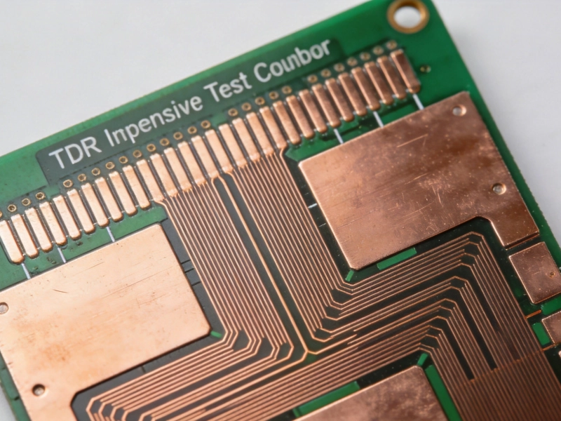
Controlled Impedance: Measuring a Manufacturer's Ability to Hit Tight TolerancesSeptember/20/2026
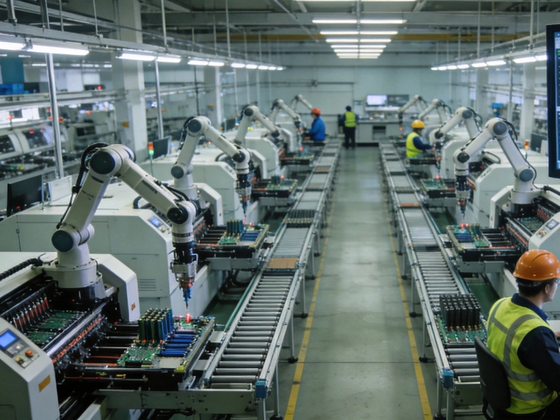
Choosing the Right Assembly Partner: Capabilities, Capabilities, Certifications, and CapacitySeptember/28/2026
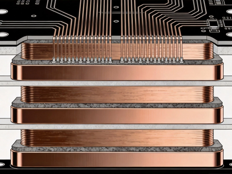
Heavy Copper PCBs: Capabilities for High-Current and Power ElectronicsJuly/14/2026
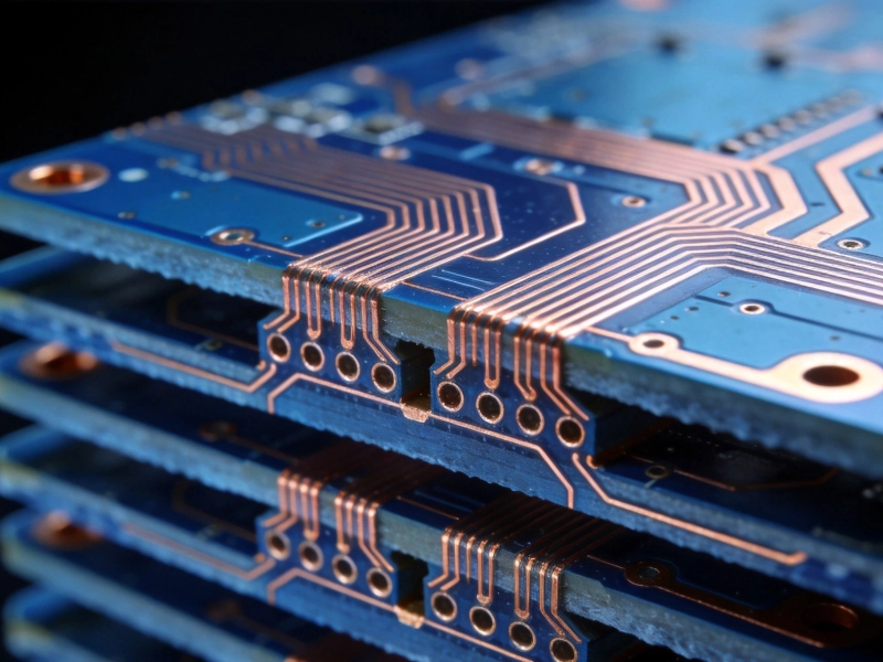
Cost Drivers in HDI and Multilayer PCB Fabrication: What Engineers Need to KnowSeptember/26/2026
The Role of Equipment in Determining PCB Fabrication Capabilities (LDI, Laser Direct Imaging)September/09/2026