Open Nav

The capabilities of a Pcb Manufacturer are fundamentally shaped by their equipment investments. While Design Rules and material selection matter, the physical machinery that transforms design files into finished boards determines what is actually achievable. Among the most transformative technologies in modern Pcb Fabrication, Laser Direct Imaging (LDI) stands out as a capability-defining investment that enables precision levels impossible with traditional Photolithography methods.
Understanding how fabrication equipment influences Manufacturing Capabilities helps engineers make informed decisions about design specifications and partner selection. This knowledge also clarifies why seemingly similar manufacturers can produce dramatically different results.
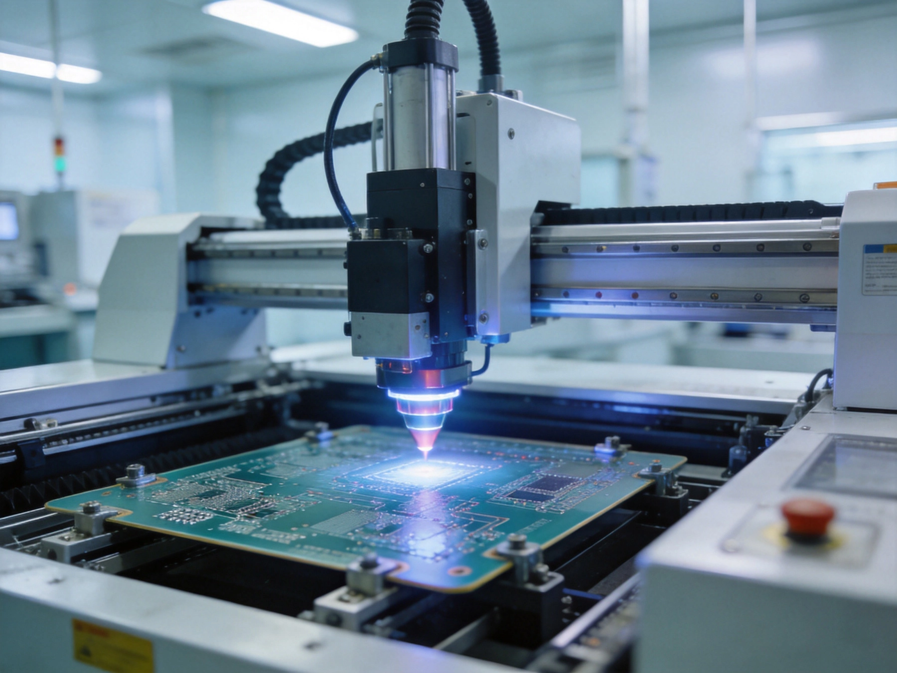
PCB imaging has evolved significantly from the early days of contact printing, where artwork films were pressed directly against photosensitive resist. While contact printing served the industry for decades, it carries inherent limitations that constrain feature resolution and registration accuracy.
Contact printing suffers from several fundamental constraints:
As PCB designs demanded finer features and tighter tolerances, contact printing reached its practical limits. Manufacturers needed alternative approaches to meet evolving requirements.
Projection imaging systems address many contact printing limitations by projecting the Circuit Pattern onto the PCB surface without physical contact. This approach reduces defects and enables better resolution but still relies on traditional artwork films as the imaging master.
Film-based projection systems improved capability but introduced new challenges. Film dimensional stability varies with temperature and humidity, limiting achievable registration accuracy. Additionally, film production itself has minimum feature limitations that cascade through the manufacturing process.
Laser Direct Imaging represents a paradigm shift in PCB imaging technology. Rather than using photographic film as an intermediate, LDI systems directly expose the Photoresist with laser beams controlled by digital design data.
LDI systems employ high-power laser sources, typically ultraviolet (UV) lasers, to directly expose Photoresist materials. The process operates as follows:
This direct digital-to-panel approach eliminates the film bottleneck entirely, enabling features and accuracies that film-based methods cannot achieve.
LDI systems utilize different laser wavelengths optimized for specific photoresist chemistries:
Most PCB-focused LDI systems operate at 355nm, balancing resolution capability with photoresist compatibility and system cost.
LDI equipment fundamentally expands what manufacturers can achieve, particularly in areas where traditional methods struggle.
LDI systems routinely achieve trace and space widths below 50 microns, with advanced systems supporting features as small as 20-30 microns. This capability opens possibilities for:
Perhaps the most significant advantage of LDI lies in registration capability. By eliminating film-based distortion and enabling real-time compensation, LDI achieves registration accuracy of 10-15 microns or better. This precision enables:
Modern LDI systems image full panels without stitching, ensuring uniform exposure across the entire board surface. This capability proves essential for:
Equipment capabilities define the manufacturing window within which designers must work. Understanding this relationship helps engineers optimize designs for producibility while pushing boundaries appropriately.
Equipment resolution directly limits minimum trace widths and spaces. LDI-equipped manufacturers can typically offer:
Traditional equipment manufacturers may quote similar specifications but achieve them with lower yield and higher cost. The difference lies in the consistency and process latitude that LDI enables.
Via annular ring dimensions depend on both imaging accuracy and drilling registration. LDI-enabled manufacturing reduces minimum annular ring requirements because:
Designers working with LDI-capable manufacturers can specify smaller annular rings without sacrificing manufacturing yield, enabling higher routing density.
LDI equipment represents significant capital investment, and manufacturers must balance capability against cost. Understanding this relationship helps buyers evaluate quotes and capabilities.
A single LDI system can cost several million dollars, with supporting infrastructure adding to the investment. Manufacturers must generate sufficient volume and margin to justify this capital outlay.
Cost factors include:
Manufacturers typically invest in LDI when their target markets require:
For simpler boards without advanced feature requirements, traditional equipment may provide adequate capability at lower cost.
When selecting a Pcb Manufacturing partner, understanding their equipment base helps predict the capabilities they can reliably deliver.
Request specific information about their imaging systems:
Reputable manufacturers document their capabilities through:
Be wary of manufacturers claiming capabilities that exceed what their equipment can achieve. If quotes seem too good to be true, probe the actual process and yield data.
Equipment capability means little without proper maintenance and process control. Understanding manufacturer quality systems helps predict the consistency you will experience.
LDI systems require regular calibration to maintain accuracy:
Ask about calibration frequency and verification procedures when evaluating manufacturers.
LDI systems operate best in tightly controlled environments:
These controls add to operating cost but are essential for achieving rated capabilities consistently.
LDI represents current capability limits, but the technology continues evolving. Understanding emerging trends helps anticipate future manufacturing possibilities.
Several developing technologies may expand capabilities further:
Modern LDI systems increasingly incorporate Industry 4.0 concepts:
These integrations improve consistency and reduce waste while enabling faster troubleshooting when issues arise.
Equipment capabilities fundamentally determine what a Pcb Manufacturer can achieve:
When specifying PCB requirements, align your Design Rules with manufacturer capabilities. Work with partners whose equipment baseline matches your precision needs. Attempting to achieve fine-feature results with inadequate equipment leads to yield issues, delays, and cost overruns.
Laser Direct Imaging (LDI) is an advanced PCB imaging technology where ultraviolet lasers directly expose photoresist on the board surface according to digital design data. Unlike traditional methods using photographic film, LDI eliminates intermediate artwork, enabling finer features and better registration accuracy.
LDI achieves finer traces because laser beams can be focused to smaller spot sizes than light passing through film. Additionally, LDI eliminates film diffraction and distortion effects, while real-time correction compensates for panel variations that would smear features in film-based processes.
LDI-equipped manufacturers typically achieve registration accuracy of 10-25 microns, with advanced systems reaching 10 microns or better. Traditional contact printing achieves 50-100 microns, and projection systems without film typically achieve 25-50 microns.
Request documentation including equipment specifications, process capability studies, and sample evaluations. Visit the facility if possible to observe the equipment. Ask specific questions about their minimum features and registration data. Reputable manufacturers welcome such inquiries.
No, LDI is most beneficial for advanced designs requiring fine features (below 100 microns), tight registration, or HDI structures. Standard designs with 200-micron traces and larger work well with traditional equipment. Paying for LDI capability on simple boards wastes budget without benefit.
Advanced equipment like LDI increases manufacturing cost through capital recovery, maintenance, and operating expenses. However, the capability it enables often justifies the premium for complex designs where traditional equipment would struggle. For high-volume simple boards, traditional equipment often provides better economics.
Minimum Trace and Space: How Far Has PCB Technology Advanced?July/01/2026
High-Frequency Materials: Assessing Capabilities for RF and Microwave PCBsAugust/03/2026
Any-Layer Interconnect: The Pinnacle of High-Density PCB TechnologyJuly/10/2026
Why Global Brands Are Turning to PCB Fabrication in China in 2026May/21/2026
Heavy Copper PCBs: Capabilities for High-Current and Power ElectronicsJuly/14/2026
Top Trends Shaping the Chinese PCB Manufacturing Industry in 2026May/21/2026
High-Frequency Materials: Assessing Capabilities for RF and Microwave PCBsJuly/23/2026
Large Format vs. Miniature PCBs: Evaluating Size Constraints and CapacitiesAugust/14/2026