Open Nav

A precision Pcb Design is only as good as the specifications that accompany it. When we review fabrication drawings for high-reliability projects, the single most common issue is not the design itself but the gap between what the engineer intended and what the documentation actually says. Tolerances that default to standard values, stack-ups that reference generic material grades without specifying thickness, impedance requirements that omit the test method — these gaps result in boards that pass inspection but fail in the field.
This article explains how to specify tolerances and layer stack-ups for custom PCBs where precision matters. We will cover what needs to be specified, why standard assumptions cause problems, and how to communicate your requirements in a way that gives your fabricator clear, actionable instructions.
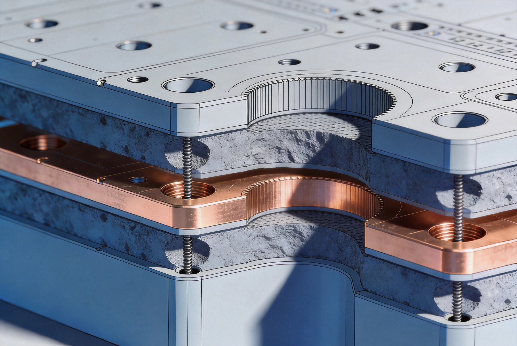
Precision in Pcb Manufacturing means the board you receive matches your design intent within defined limits. It does not mean the tightest possible tolerance on every parameter — that is a recipe for unnecessary cost and low yield. Precision means each tolerance is appropriate to the application, clearly stated, and verifiable through measurement.
A precise specification package contains three elements: the nominal value, the acceptable tolerance range, and the verification method. For example, stating "impedance 50 ohms" is not a specification. Stating "impedance 50 ohms differential, tolerance plus or minus 10 percent, verified by TDR on test coupon with stack-up matching production layers" is a specification. The difference is measurable.
When we work with engineers on Custom Pcb projects, the most productive early conversation is about which tolerances drive their design and which ones can default to standard values. Tightening a tolerance that does not matter adds cost without benefit. Leaving a critical tolerance unspecified risks a functional failure. The art of precision specification is knowing which parameters need explicit definition and which ones can stay on the standard process window.
The stack-up is the architectural blueprint of a Multilayer Pcb. It defines layer count, layer ordering, copper weight on each layer, dielectric material and thickness between layers, and the overall finished board thickness. Every one of those parameters has a tolerance, and for precision boards, those tolerances need to be explicit.
Start with the substrate material. Standard FR-4 is a category, not a specific material. Different manufacturers produce FR-4 grades with different glass transition temperatures (Tg), dielectric constants (Dk), and loss tangents (Df). For boards that operate at high frequency, high temperature, or in thermally cycled environments, specifying the exact material grade is essential.
High-speed designs often require low-loss materials with tightly controlled Dk. Standard FR-4 has a Dk tolerance around plus or minus 10 percent. High-performance materials like Rogers RO4000 series or Isola I-Tera achieve Dk tolerances of plus or minus 2 percent or better. If your impedance budget depends on stable Dk, you need to specify the material by manufacturer and grade, not just by generic name.
For thermal performance, specify the minimum Tg requirement. Standard FR-4 grades range from 130 degrees Celsius to 140 degrees Celsius. High-Tg materials exceed 170 degrees Celsius. Polyimide and ceramic-filled materials go even higher. The thermal performance of your board in lead-free assembly and in service depends on this choice, so make it explicit in your stack-up table.
Dielectric thickness between layers directly affects impedance and Signal Integrity. Prepreg and core thicknesses have manufacturing tolerances that vary by material and construction. Standard Prepreg thickness tolerance is approximately plus or minus 10 percent. For Controlled Impedance traces, that variation can push impedance outside the acceptable range even if trace width is perfectly controlled.
For precision impedance requirements, specify a tighter thickness tolerance — typically plus or minus 5 percent or less — and confirm with your fabricator that their process can achieve it. This may require using spread-glass or no-flow prepregs rather than standard woven glass constructions, which affects both cost and availability.
Copper weight on each layer affects current capacity, thermal performance, and impedance. Standard copper weights are 0.5 ounce, 1 ounce, and 2 ounce per square foot. For power layers or heavy current paths, specify 2 ounce or heavier. For fine-line impedance layers, specify 0.5 ounce or even 0.25 ounce to achieve tighter trace width control.
Copper distribution across the panel matters too. Balanced copper distribution — similar copper area on adjacent layers — reduces warpage during lamination and assembly. If your design has heavily asymmetrical copper distribution, note it in your stack-up drawing and discuss with your fabricator whether panel-level adjustments can improve yield.
Dimensional tolerances govern how well the board fits into its enclosure and how precisely features align across layers. The most important categories are board outline, hole position, and layer registration.
Board outline tolerance is typically plus or minus 0.2 millimeter for standard routed panels. For boards that must fit into precision-machined housings, specify a tighter tolerance such as plus or minus 0.1 millimeter or plus or minus 0.05 millimeter. Routed edges have different tolerances than scored or V-scored panel edges, so specify the edge finish as well.
Board thickness tolerance includes both the stack-up thickness and the surface finish thickness. Standard thickness tolerance is plus or minus 10 percent. For connector interfaces where Z-height matters, specify both the nominal thickness and the acceptable range explicitly.
Drill position tolerance describes how accurately the drilled hole locations match the pattern on each layer. Standard tolerance is plus or minus 0.075 millimeter for mechanical drilling. For tight-pitch BGAs or fine-line designs, specify a tighter tolerance such as plus or minus 0.05 millimeter or plus or minus 0.025 millimeter.
Finished hole size tolerance includes both the drill diameter and the plating thickness. A 0.3 millimeter drill with 25 micron copper plating yields a finished hole around 0.25 millimeter. If your design depends on specific finished hole sizes for press-fit connectors or other applications, specify finished hole size with tolerance, not just drill size.
Layer registration tolerance describes how precisely features on different layers align with each other. This is often the most misunderstood tolerance in precision PCBs. Standard registration tolerance ranges from plus or minus 0.1 millimeter to plus or minus 0.15 millimeter depending on layer count and panel size. For HDI designs or fine-pitch components, specify tighter registration — plus or minus 0.05 millimeter or better — and discuss with your fabricator whether their equipment can achieve it.
Controlled Impedance is one of the most common precision requirements in modern PCBs. Yet impedance specifications are frequently incomplete, leading to test results that do not match the design intent.
Specify the target impedance value and the acceptable tolerance. Standard impedance tolerance is plus or minus 10 percent to plus or minus 15 percent. For high-speed differential pairs at data rates above 5 gigabits per second, tighter tolerance — plus or minus 5 percent or plus or minus 7 percent — is often necessary. Do not assume tighter is always better. Tighter impedance tolerance increases fabrication cost and reduces yield. Match the tolerance to your actual signal margin.
Impedance is verified on a test coupon that runs alongside the production panel. The coupon must match the production stack-up in layer order, material, and trace geometry. Specify that the coupon design matches your impedance traces exactly — trace width, copper weight, and reference plane distance. A coupon that uses a different stack-up will give you a number, but not a number that represents your actual traces.
Specify the measurement method. Time-domain reflectometry (TDR) is the standard method for high-speed digital impedance verification. Cross-section analysis is used for destructive verification of trace geometry. State whether you require TDR testing on 100 percent of panels or statistical sampling. For high-reliability applications, 100 percent TDR testing is worth the additional cost.
Surface finish affects solderability, contact resistance, and long-term reliability. Each finish type has characteristic thickness ranges and tolerances.
ENIG is the most common finish for precision boards. Standard ENIG has approximately 3 to 5 microinches of gold over 100 to 150 microinches of nickel. For applications where contact resistance or insertion cycles matter, specify minimum nickel thickness of 120 microinches and minimum gold thickness of 3 microinches. Thicker nickel prevents black-pad syndrome; thicker gold improves contact durability.
For edge connectors and high-cycle contact surfaces, hard gold is preferred. Hard gold plating thickness ranges from 10 to 50 microinches over nickel. Specify the minimum gold thickness for your contact requirement. For 500 or more mating cycles, 30 microinches is typical. For 1000 cycles or more, 50 microinches may be required.
Immersion tin, immersion silver, and OSP each have specific use cases. Immersion tin works well for aluminum wire bonding. Immersion silver offers good solderability at moderate cost. OSP is economical but limited to single-reflow applications. Specify finish type and minimum thickness where contact performance is critical.
Solder Mask registration affects how precisely the mask covers adjacent traces and defines exposed pad areas. Standard mask registration tolerance is plus or minus 0.05 millimeter to plus or minus 0.1 millimeter. For fine-pitch components where mask encroachment on pads is a concern, specify tighter registration tolerance.
Legend or Silkscreen registration follows similar principles. Standard tolerance is plus or minus 0.1 millimeter. For boards where component marking precision affects assembly or field service, specify the required registration accuracy.
Board flatness matters for assembly and for fit into enclosures. Standard bow and twist limits are defined in IPC-6012 as 1.0 percent to 1.5 percent of the board diagonal depending on thickness. For Smt Assembly with fine-pitch components or boards that mount flush to a chassis, specify tighter limits — for example, maximum 0.5 percent bow and twist.
Coplanarity of component mounting surfaces is critical for BGA assembly. If your design uses large BGAs on a board that may exhibit warpage, discuss the flatness requirement with your fabricator and specify it explicitly.
For precision boards, the specification package should include verification requirements. This defines what data you will receive from the fabricator to confirm the board meets your tolerances.
Request cross-section photographs for the first article of any new design. Cross-section shows actual layer thicknesses, plating quality, and hole wall integrity. It is the definitive verification of stack-up construction.
Request TDR test data from the production coupon. The data should include measured impedance values, tolerance assessment, and identification of any traces that fall outside the specified range.
For boards with critical outline or hole position tolerances, request CMM (coordinate measuring machine) data or coordinate measurement verification. This confirms the board matches your dimensional specification.
The fabricator is your partner in achieving precision, not just a vendor executing a drawing. Engage them early, especially on new designs with tight tolerances. An experienced fabricator can flag potential tolerance conflicts, suggest design adjustments that improve yield, and confirm which tolerances are achievable on their equipment.
Before finalizing your specification, review it with your fabricator's engineering team. Confirm that the tolerances you are specifying are within their standard capability window. If a tolerance requires special process control, understand the cost and lead time impact. This conversation prevents surprises on the production floor.
For ongoing production of precision boards, establish a process for regular capability review. Tolerances that were achievable last year may shift as equipment ages, materials change, or personnel turnover occurs. Regular dialogue keeps your specifications aligned with actual process capability.
For 10 Gbps differential signaling, plus or minus 5 percent to plus or minus 7 percent impedance tolerance is typical. Tighter tolerance improves signal margin but increases fabrication cost. Work with your Signal Integrity engineer to determine the minimum acceptable impedance window based on your driver and receiver characteristics.
Ask for their process capability data sheet. A reputable fabricator can provide statistical process capability data for registration, drill position, Impedance Control, and other key parameters. If they cannot provide capability data, that tells you something important about their process maturity.
It depends on your frequency and thermal requirements. For high-speed digital above 5 Gbps, RF designs above 1 GHz, or boards that operate at elevated temperature, high-performance materials with controlled Dk and Df are worth the additional cost. For lower-frequency designs or boards that operate near room temperature, standard high-Tg FR-4 is typically sufficient.
Drill tolerance describes the mechanical accuracy of the drilling process. Finished hole tolerance includes both drill tolerance and plating thickness variation. If your design depends on specific hole sizes for connectors, press-fit components, or other mechanical requirements, specify finished hole size with tolerance, not just drill size.
State-of-the-art precision fabricators can achieve registration tolerances of plus or minus 0.025 millimeter on layer counts up to 10 to 12 layers. Higher layer counts and larger panel sizes generally have looser registration capability. For HDI designs with sequential build-up layers, each lamination cycle adds cumulative registration variation, so discuss the specific layer stack-up with your fabricator.

Comparing Traditional vs. Digital Quick Turn PCB ServicesJuly/18/2026

Why Quick Turn PCB Fabrication is Critical for R&D TeamsMay/21/2026

How AI-Driven Scheduling is Making Rapid PCB Prototyping More ReliableJune/18/2026
Managing Signal Integrity and Impedance Control in High-Speed Multilayer PCBsJuly/21/2026

Emergency PCB Runs: Strategies for Getting Boards Fast Without Sacrificing ReliabilityJuly/08/2026

24-Hour Turnaround: Is it Possible and How Does it Work?May/21/2026
Demystifying Layer Lamination: How Multilayer Boards are BuiltJune/05/2026

How Automation is Revolutionizing China's PCB SectorJune/03/2026