Home Blog PCB Fabrication Solutions Automotive & EV Systems

Testing Services: From Flying Probe to Functional Testing (FCT)

August/15/2026

Quality assurance in Electronics Manufacturing relies on a multi-layered testing strategy that catches defects at various stages of production. From initial bare board verification to comprehensive functional validation, each testing method serves a specific purpose in ensuring that assembled PCBs meet design specifications and performance requirements.

This article explores the complete spectrum of PCB testing services, from the versatile flying probe testing used for prototypes and small batches, through in-circuit testing for manufacturing defects, to fully automated functional testing that validates real-world performance. Understanding these testing options helps manufacturers build quality assurance strategies appropriate for their product complexity, volume requirements, and reliability standards.

Testing Services: From Flying Probe to Functional Testing (FCT)

The Testing Hierarchy: A Strategic Overview

Effective quality assurance requires testing at multiple levels, with each tier catching different defect types:

  • Electrical Testing – Verifies connectivity and component values
  • Parametric Testing – Validates component tolerances and analog performance
  • Functional Testing – Confirms circuit operation under realistic conditions

No single test method catches all defects. A comprehensive strategy combines multiple approaches appropriate to production volume, product complexity, and quality requirements.

Flying Probe Testing: Flexible First-Line Defense

How Flying Probe Testing Works

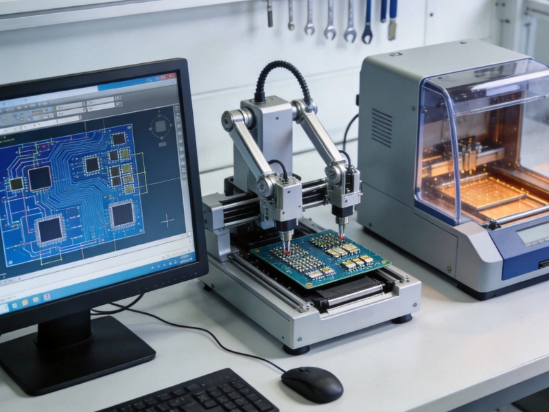
Flying probe testers use movable test probes that make temporary electrical contact with test points on the PCB surface. Unlike fixture-based testers that require custom bed-of-nails fixtures, flying probes navigate the board programmatically, touching down at specified locations to perform electrical measurements.

Modern flying probe systems feature:

  • High-precision positioning – Sub-mil accuracy for fine-pitch components
  • Multiple probe heads – Typically 4-8 probes for parallel testing
  • Fast travel speeds – High-velocity positioning reduces test time
  • Flexible programming – No physical fixtures required for new designs

Advantages of Flying Probe Testing

Flying probe testing offers unique benefits for specific manufacturing scenarios:

  • No fixture costs – Eliminates expensive bed-of-nails fixture fabrication
  • Quick setup – Programming from CAD data, minimal changeover time
  • Design flexibility – Ideal for prototypes and frequent design changes
  • Low volume economics – Cost-effective for small batch production
  • Accessible test points – Can reach areas difficult for fixture-based testing

Limitations and Considerations

While versatile, flying probe testing has constraints:

  • Slower throughput – Serial probe movements limit test speed
  • Non-powered testing – Cannot test active components in-circuit
  • Contact limitations – Requires accessible test points on board surface
  • Component stress – Physical contact risks damage to sensitive components

Flying probe excels in Prototype validation, low-volume production, and situations requiring maximum flexibility.

Bed-of-Nails In-Circuit Testing (ICT)

ICT Fundamentals

In-circuit testing uses a custom fixture populated with spring-loaded test pins arranged to contact specific test points on the PCB simultaneously. When the board is loaded into the fixture, hundreds or thousands of pins make contact, enabling comprehensive Electrical Testing in seconds.

ICT systems verify:

  • Component presence – Correct parts in correct positions
  • Component value – Resistance, capacitance, inductance measurements
  • Solder joint quality – Opens, shorts, and marginal connections
  • Polarity verification – Correct orientation of diodes, capacitors, ICs
  • Analog performance – Basic parametric checks on active devices

ICT Fixture Investment

The primary barrier to ICT implementation is fixture cost and lead time:

  • Fixture fabrication – Typically $5,000-$50,000 depending on complexity
  • Lead time – 2-6 weeks for fixture design and manufacturing
  • Design stability requirement – Fixtures are design-specific
  • Maintenance – Spring pins wear and require periodic replacement

These factors make ICT most economical for stable, high-volume production where fixture costs amortize across many units.

ICT Test Coverage

Maximizing ICT coverage requires Design for Testability (DFT) considerations during Pcb Layout:

  • Test point placement – Strategic location of accessible test pads
  • Component spacing – Adequate clearance for test probe access
  • Boundary scan integration – JTAG interfaces for digital device testing
  • Isolation strategies – Ability to disable analog devices for digital testing

Well-designed boards can achieve 90%+ component coverage with comprehensive ICT.

Boundary Scan Testing (JTAG)

JTAG Technology Overview

Boundary scan, defined by IEEE 1149.1 (JTAG), provides digital test access through a standardized serial interface. Instead of requiring physical probe access to device pins, boundary scan places test cells at each digital I/O, allowing test patterns to be shifted in and test results shifted out.

JTAG capabilities include:

  • Interconnect testing – Verifies traces between JTAG-capable devices
  • Device programming – In-system programming of FPGAs, CPLDs, microcontrollers
  • Built-in self-test – Access to internal device test features
  • Cluster testing – Testing non-JTAG devices surrounded by JTAG devices

JTAG Implementation Benefits

Boundary scan offers significant advantages for complex digital boards:

  • Reduced test point requirements – Fewer physical access points needed
  • BGA testing – Access to hidden pins under ball grid arrays
  • High-density board support – Tests where physical access is impossible
  • Reusable test infrastructure – Standard interface across devices

JTAG Integration with Other Methods

JTAG rarely stands alone but enhances overall test strategy:

  • JTAG + ICT – Boundary scan for digital, ICT for analog components
  • JTAG + Functional – Structural test before functional validation
  • JTAG programming – Device configuration before functional testing

Automated Optical Inspection (AOI)

AOI in the Testing Continuum

While AOI doesn't perform electrical tests, it serves as a critical early defect detection method that reduces the burden on subsequent electrical testing. By catching visible defects before electrical testing, AOI prevents unnecessary test time on obviously defective boards.

AOI detects:

  • Component defects – Wrong part, missing part, reversed polarity
  • Solder defects – Insufficient, excessive, bridging, opens
  • Placement errors – Offset, rotated, lifted components
  • Physical damage – Scratches, contamination, delamination

AOI Placement Strategy

Strategic AOI placement optimizes defect detection cost-effectiveness:

  • Post-reflow – Most common placement for solder joint inspection
  • Pre-reflow – Catches placement errors before soldering
  • Post-wave – For mixed-technology boards with through-hole components

X-Ray Inspection

When X-Ray is Essential

Automated X-Ray Inspection (AXI) examines solder joints hidden beneath component bodies. For BGA, QFN, and other bottom-terminated components, X-ray is the only non-destructive method to verify solder connection quality.

X-ray inspection reveals:

  • Void analysis – Excessive voids in thermal pads reduce reliability
  • Bridging – Shorts between adjacent balls or pads
  • Insufficient solder – Inadequate ball or paste volume
  • Component alignment – Shifted or rotated components
  • Head-in-pillow – Ball and paste not properly fused

2D vs. 3D X-Ray

  • 2D X-ray – Single angle projection, suitable for simple analysis
  • 3D X-ray ( laminography/CT) – Cross-sectional views, better for complex boards

Functional Circuit Testing (FCT)

The Ultimate Validation

Functional testing represents the final verification that an assembled PCB operates correctly in its intended application. Unlike structural tests that verify component presence and connectivity, FCT exercises the board under realistic operating conditions, measuring performance against design specifications.

FCT typically includes:

  • Power-up verification – Correct voltage levels and sequencing
  • Digital functional tests – Logic verification, communication interfaces
  • Analog performance – Signal quality, accuracy, frequency response
  • Calibration procedures – Adjusting trim components to meet specifications
  • Environmental loading – Testing under temperature, load, or stress conditions

FCT Fixture Design

Functional test fixtures are typically more complex than ICT fixtures:

  • Interface connections – Connectors for power, signals, and communication
  • Load simulation – Resistive, capacitive, or inductive loads as appropriate
  • Sensor integration – Temperature, voltage, current measurement points
  • RF considerations – Shielding and Impedance Control for high-frequency circuits

FCT Program Development

Developing comprehensive FCT programs requires:

  • Test specification – Clear pass/fail criteria for each test
  • Test sequence – Logical order preventing damage to untested sections
  • Fault isolation – Diagnostic capability to identify failure locations
  • Data logging – Recording test results for quality tracking

Selecting the Right Testing Strategy

Volume Considerations

Production volume significantly influences test method selection:

  • Prototypes (1-10 units) – Flying probe, manual testing, limited AOI
  • Low volume (10-1000) – Flying probe, AOI, selective functional test
  • Medium volume (1000-10000) – ICT consideration, comprehensive AOI, FCT
  • High volume (10000+) – ICT with full fixture investment, automated FCT

Product Complexity Factors

Board characteristics guide testing emphasis:

  • Digital-heavy designs – JTAG, ICT for connectivity, functional for integration
  • Analog precision circuits – Parametric testing, calibration verification
  • RF/wireless – Specialized RF functional testing, spectrum analysis
  • High-reliability – Comprehensive coverage with multiple test levels
  • High-density BGAs – X-ray inspection essential

Quality and Reliability Requirements

Application requirements dictate test thoroughness:

  • Consumer electronics – AOI + basic functional test
  • Industrial controls – ICT + comprehensive FCT
  • Medical devices – Complete traceability, 100% test coverage
  • Aerospace/military – Multiple test levels with full documentation

Test Strategy Integration

The Complete Testing Continuum

A comprehensive test strategy sequences methods for maximum effectiveness:

  1. AOI (Post-reflow) – Catch visible defects early
  2. X-ray (if BGAs/QFNs) – Verify hidden solder joints
  3. Flying Probe or ICT – Electrical connectivity and component verification
  4. Boundary Scan – Digital structural test (if applicable)
  5. Functional Test – Performance validation under operating conditions
  6. Burn-in (if required) – Extended operation to precipitate early failures

Test Data Integration

Modern manufacturing systems integrate test data across methods:

  • Unified data collection – All test results in central database
  • Defect correlation – Linking AOI findings to ICT failures to FCT results
  • Trend analysis – Statistical process control across test stages
  • Traceability – Complete test history for each serialized board

Advanced Testing Technologies

Automated Test Generation

Modern tools automate test program development:

  • CAD-integrated test point selection – Automated DFT analysis
  • Test program generation – Software-created ICT and flying probe programs
  • Model-based testing – Simulation-derived functional test vectors

Machine Learning in Test

Emerging AI applications enhance testing:

  • Defect classification – Automated AOI false-call reduction
  • Predictive analytics – Identifying boards at risk of future failure
  • Adaptive testing – Dynamic test prioritization based on defect patterns

Cost-Effectiveness Considerations

Test Investment vs. Risk

Testing strategy balances prevention cost against failure cost:

  • Escaped defect cost – Warranty, repair, reputation damage
  • Test cost per unit – Equipment, programming, operation
  • Opportunity cost – Test time vs. production throughput
  • Fixture amortization – Volume required to justify fixture investment

Test Escapes and Coverage Analysis

Continuous improvement requires analyzing test effectiveness:

  • Field failure analysis – Identifying defects missed by testing
  • Coverage improvement – Adding tests for escaped defect types
  • Test optimization – Removing redundant tests, adding missing coverage

Conclusion

Effective PCB testing requires a strategic approach combining multiple methods appropriate to production volume, product complexity, and quality requirements. From the flexibility of flying probe testing for prototypes to the comprehensive validation of functional testing for production units, each method contributes to overall quality assurance.

The most successful manufacturers view testing not as a cost center but as an investment in customer satisfaction and brand reputation. By implementing the right testing strategy—whether that's flying probe for Rapid Prototyping, ICT for high-volume manufacturing, or comprehensive FCT for mission-critical applications—companies ensure their products meet the performance and reliability standards their customers demand.

As electronics continue increasing in complexity while decreasing in size, testing technology evolves to meet these challenges. Staying current with testing capabilities and integrating them effectively into manufacturing workflows remains essential for competitive electronics production.

Comprehensive Testing Services for Your PCBs

From flying probe testing for prototypes to full functional validation for production, our testing services ensure your boards meet the highest quality standards. Contact us to discuss your testing requirements and build a quality strategy that fits your product needs.

Frequently Asked Questions

What is the difference between ICT and functional testing?

ICT (In-Circuit Testing) checks individual components and connections without powering the board, verifying component values and solder joints. Functional testing powers the board and validates operation under realistic conditions, confirming the circuit performs its intended function.

When should I choose flying probe over ICT?

Flying probe testing is ideal for prototypes, low-volume production, and designs undergoing frequent changes where ICT fixture costs cannot be justified. ICT becomes economical for stable, high-volume designs where fixture costs amortize across thousands of units.

Can I skip AOI if I have ICT or functional testing?

While electrical testing can catch many defects, AOI catches visible defects before electrical testing, preventing wasted test time on obviously defective boards. AOI also detects defects like component polarity errors that might pass electrical tests but cause field failures.

What test coverage should I aim for?

Coverage targets depend on application requirements: consumer electronics may accept 80% coverage, while medical or aerospace applications typically require 95%+ coverage with full traceability. Work with your contract manufacturer to establish appropriate targets.

How does JTAG testing complement other methods?

JTAG (boundary scan) provides access to digital device pins without physical probe contact, enabling testing of BGA and high-density components where physical access is impossible. It complements ICT and functional testing by providing structural digital testing capabilities.
Send Message
Name*
E-mail*
Country*
Phone/WhatsApp*
Name*
E-mail*
Country*
Phone/WhatsApp*