Open Nav

When your smartphone drops a call, your car's airbag fails to deploy, or industrial equipment shuts down unexpectedly, you probably don't think "ionic contamination on the PCB." But these invisible residues—the remnants of solder flux, fingerprints, and processing chemicals—cause a surprising number of electronic failures. The chemistry of what remains on your circuit board after assembly can mean the difference between a product that lasts a decade and one that fails in months.
This article dives deep into the science of PCB contamination: what it is, how it forms, why it matters, and how to control it through proper cleaning processes.
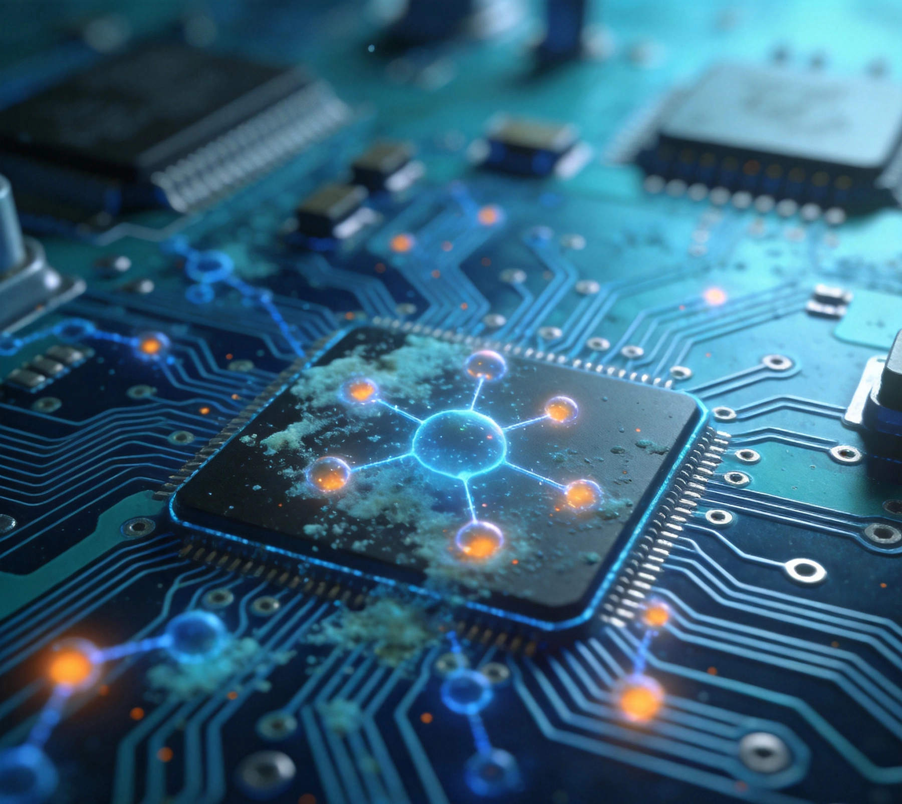
Ionic contamination refers to ionizable residues on a PCB surface. These are not visible to the naked eye—in most cases, you can't see the contamination that's causing reliability problems. But these charged particles, whether from flux residues, salts, acids, or alkalis, become conductive when moisture is present, creating leakage pathways that can short circuit signals or corrode metal surfaces.
The term encompasses a wide range of chemical species:
Understanding why ionic contamination causes failures requires some basic electrochemistry. When water accumulates on a PCB surface—whether from humidity, condensation, or immersion—it dissolves ionic residues into conductive electrolyte solutions. This creates the conditions for several failure mechanisms.
Imagine two adjacent traces at different voltages. Under dry conditions, the air gap between them provides excellent isolation. But when ionic contamination is present and moisture adsorbs to the surface, a conductive water film forms. Ions migrate between the traces, creating measurable leakage current that can:
Perhaps the most insidious failure mechanism is electrochemical migration, sometimes called dendrite growth. When an electric field is present across a contaminated surface, metal ions dissolve from the more electronegative trace and deposit on the opposite electrode, forming conductive filaments that bridge the gap.
The classic example is silver migration: silver traces under bias in the presence of moisture and halides form dendritic growths that can bridge between conductors, causing short circuits. But copper, tin, and lead can all migrate under the right conditions.
Dendrites typically grow slowly over months or years—often just enough to pass initial testing but fail in the field. This makes them particularly dangerous for applications where reliability is critical: medical devices, automotive electronics, aerospace systems.
Similar to migration but distinct, creep corrosion occurs when corrosion products spread beyond the initial site. On PCBs with contaminated surfaces, the corrosion of copper traces can produce copper compounds that migrate across the surface, creating conductive pathways that grow over time.
Ionic contamination beneath components or within the PCB substrate can accelerate delamination. Water-reactive compounds weaken the interface between copper and substrate, creating voids that compromise mechanical integrity and thermal performance.
Contamination can enter your process at multiple points. Understanding these sources helps you build effective controls.
Flux is the primary culprit in most Pcb Assembly contamination. Whether you're using rosin-based, water-soluble, or no-clean fluxes, residues remain on the board after soldering. The composition and cleanability of these residues varies dramatically:
Human skin oils contain sodium, potassium, and other ionic species. Every fingerprint on a PCB leaves a contamination trail. While flux cleaners can remove some of this contamination, thorough cleaning requires proper handling protocols: gloves, clean work surfaces, and minimal board touching.
Plating solutions, etching chemicals, developer solutions, and rinsing water can all leave contamination if not properly managed. Even "pure" water can introduce contamination if it contains dissolved ions—deionized water is essential for final rinsing.
In manufacturing environments, airborne particulate and gaseous contaminants can settle on boards. Salt fog testing (common in automotive and marine applications) explicitly tests the board's ability to withstand chloride contamination from atmospheric exposure.
Component leads and termination surfaces can carry contamination from their manufacture or storage. Plating chemicals, mold release agents, and storage preservatives can all transfer to the PCB during assembly.
Pcb Cleaning is fundamentally about dissolving and removing contamination. Understanding the chemistry helps you select the right process and avoid creating new problems.
Solvent cleaners work by dissolving hydrophobic contaminants—flux rosin, oils, greases. Common solvent families include:
The limitation of pure solvent cleaning is that it doesn't remove polar (water-soluble) contaminants. Many flux residues contain both hydrophobic and hydrophilic components.
Water-based cleaning uses detergents, saponifiers, or combinations to remove contamination. The chemistry involves:
Aqueous cleaning requires proper rinsing and drying. Residual detergent can itself be a contamination source. Water spots—mineral deposits from drying water—can create reliability issues.
Semi-aqueous processes combine solvent pre-wash with aqueous cleaning. The solvent removes heavy soils (including some difficult-to-clean residues) while the aqueous step removes polar contamination and the solvent residues themselves.
This approach balances cleaning effectiveness with environmental and safety concerns. Many no-clean fluxes that resist pure aqueous cleaning perform well with semi-aqueous processes.
Mechanical energy enhances cleaning by:
However, ultrasonic energy can damage sensitive components, particularly ceramic capacitors and certain MEMs devices. The frequency and power must be carefully selected. Many manufacturers limit or prohibit ultrasonic cleaning near specific component types.
You can't control what you can't measure. Several test methods assess PCB cleanliness.
SIR testing measures the resistance between interdigitated test patterns on a coupon board. After exposure to temperature/humidity conditions, low resistance indicates ionic contamination or other surface issues.
IPC-TM-650 Method 2.6.3 provides the standard test procedure. Pass/fail thresholds depend on application: automotive typically requires >100 MΩ between test cycles, while less demanding applications may accept lower values.
Ion chromatography identifies and quantifies specific ionic species extracted from board surfaces. The process involves:
Results are reported in μg/in² (or μg/cm²) of equivalent sodium chloride. IPC specification typically cites <1.5 μg/in² NaCl equivalent as acceptable for most applications, though critical applications may require much lower levels.
ROSE testing (also called cleanability testing) measures the resistivity of solvent that has washed a board. Lower resistivity indicates more dissolved ionic contamination. This quick test provides a pass/fail indication but doesn't identify specific contaminants.
While ionic contamination is invisible, visual inspection can reveal other cleanliness issues: flux spattering, solder balls, fibers, and other debris that may trap or indicate contamination. 100x-200x microscopy is standard for process monitoring.
Effective cleaning requires attention to the entire process, not just the cleaning chemistry.
The condition of boards entering the cleaner affects process performance:
Beyond chemistry, process parameters determine cleaning effectiveness:
Clean boards are vulnerable to recontamination:
In some applications, cleaning alone cannot provide sufficient protection. Conformal coatings—thin polymer layers applied over the assembled PCB—provide additional barriers against moisture and contamination.
But cleaning before coating is absolutely essential. Any contamination trapped beneath a Conformal Coating becomes concentrated as moisture diffuses through the coating and collects at the contamination sites. This accelerates rather than prevents failure.
Coating application processes (masking, application, curing) introduce their own contamination risks, requiring careful process control and often additional cleaning steps after coating.
Cleanliness requirements vary dramatically by application.
Automotive standards (ISO 16750, AEC-Q200) specify stringent cleanliness requirements due to the harsh operating environment: temperature extremes, humidity, vibration, and road chemicals. SIR testing under biased conditions is standard qualification practice.
Medical electronics must withstand sterilization processes and body fluid exposure. Surface insulation resistance requirements are particularly stringent. Many medical devices require cleaning followed by Conformal Coating or potting.
MIL-PRF-38510 and similar standards specify cleanliness levels for military and aerospace electronics. Extended humidity testing and salt fog exposure are common qualification requirements.
Consumer products face cost pressure that limits cleaning investments. No-clean processes and minimal cleaning are common, with reliability requirements tailored to product life expectancy and operating environment.
Industrial controls, Power Electronics, and infrastructure equipment often operate in uncontrolled environments with wide temperature swings and potential moisture exposure. Moderate cleanliness requirements with SIR verification are typical.
Several trends are shaping Pcb Cleaning practices:
Environmental concerns continue to drive away from harsh solvents (CFCs, perfluorinated compounds) and toward more benign alternatives. Water-based and bio-based cleaning chemistries are gaining market share.
As components shrink and pitches decrease, cleaning becomes more challenging. Beneath BGAs and beneath CSPs, traditional spray or immersion cleaning may not reach. New technologies—vapor phase, cryogenic, and supercritical CO2 cleaning—are emerging to address these needs.
Lead-free solder adoption has introduced new cleaning challenges. Lead-free fluxes often have higher melting temperatures and leave more tenacious residues. Higher copper content in lead-free alloys increases corrosion concerns. Cleaning processes must adapt to these changes.
The chemistry of PCB cleaning is complex, but the underlying principle is simple: contamination causes failures. Ionic residues create leakage pathways, enable migration, and accelerate corrosion. In applications where reliability matters, controlling contamination through proper cleaning is not optional—it's essential.
The right cleaning process depends on your specific situation: the flux system you're using, the components on your board, your reliability requirements, and your manufacturing environment. But whatever process you choose, measuring cleanliness and maintaining process control are non-negotiable.
When you consider that the cost of a field failure—in warranty returns, reputation damage, and liability—far exceeds the cost of proper cleaning, the economics become clear. Invest in cleanliness. Your customers' products will thank you.
IPC guidelines typically cite <1.5 μg/in² NaCl equivalent for general electronics. Critical applications (automotive, medical, aerospace) may require <0.5 μg/in² or lower. The right threshold depends on your application, operating environment, and reliability requirements.
"No-clean" means the flux doesn't require cleaning for most applications—it leaves minimal visible residue. However, ionic contamination can still be present, and for high-reliability applications, cleaning may still be beneficial or required. Evaluate your specific reliability requirements.
Regular cleanliness testing using SIR measurements or ion chromatography provides objective data. Establish baseline measurements, monitor process capability, and investigate any trend toward higher contamination levels before you exceed acceptable limits.
Ultrasonic energy can damage certain components, particularly ceramic capacitors, piezoelectric sensors, and MEMs devices. Always verify component compatibility. Lower frequencies (20-40 kHz) are more aggressive; higher frequencies (120 kHz+) are gentler but may clean less effectively.
Potential consequences include: increased surface leakage current, intermittent operation due to moisture adsorption, dendritic growth causing field failures, accelerated corrosion, reduced insulation resistance, and premature failure in humid or wet environments. The specific failure mode depends on the contamination level and application stress factors.
Need help optimizing your PCB cleaning process? Our engineering team can analyze your contamination risks and recommend appropriate cleaning and testing protocols.
Quality Control 101: AOI, X-Ray, and Electrical Testing in PCB ProductionAugust/10/2026
Visualizing the Flow: An Infographic Guide to How Your PCB is MadeSeptember/24/2026
Is PCB Fabrication in China Still the Most Cost-Effective Option? A 2026 AnalysisJuly/27/2026
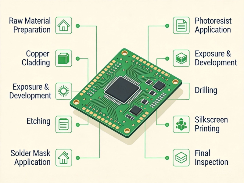
A Step-by-Step Walkthrough of the PCB Fabrication ProcessMay/21/2026
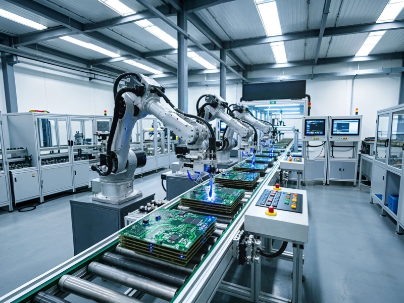
How Automation is Revolutionizing China's PCB SectorJune/03/2026
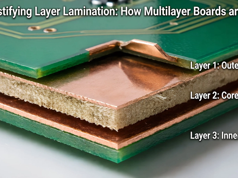
Demystifying Layer Lamination: How Multilayer Boards are BuiltJune/05/2026
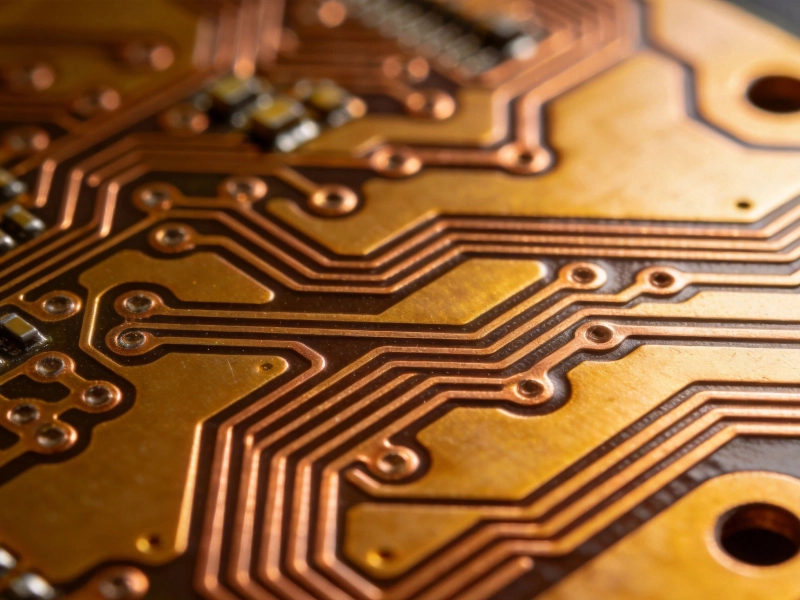
Understanding Copper Plating: Ensuring Connectivity and Durability in PCBsJuly/09/2026
Surface Preparation: The Critical Steps Before Component AssemblySeptember/16/2026