Open Nav

You upload your Gerber Files, wait a few days, and a finished PCB arrives at your door. But what actually happens in between? Understanding the manufacturing process—really understanding it, step by step—makes you a better designer. When you know how copper is etched, why lamination pressure matters, or what a drill file tells the CNC machine, you make design decisions that reduce cost, improve yield, and avoid the frustrating surprises that delay projects.
This guide walks through the complete PCB Fabrication process from raw materials to finished board, explaining what happens at each stage, why it matters, and what you can do as a designer to make the process go smoothly.
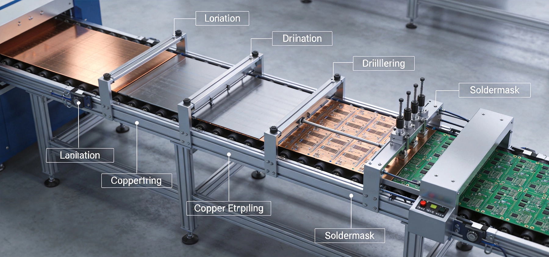
Every PCB starts as a copper-clad laminate—a sheet of dielectric material (most commonly FR-4 epoxy-glass) with thin copper foil bonded to one or both sides. The laminate grade, copper weight, and thickness are specified by the designer and must match the requirements of the finished board.
The fabricator selects the appropriate laminate from inventory based on your stackup specification. For Multilayer Boards, different laminate thicknesses and Prepreg (pre-impregnated glass-epoxy) sheets are combined to build the total stackup. The raw laminate is cut into panels—typically 18×24 inches or 21×24 inches—large enough to hold multiple copies of your board (panelization) plus tooling borders for handling during manufacturing.
For Multilayer Boards, the inner layer circuit patterns must be created first. This is where your Gerber data is converted into the physical copper patterns on the laminate.
The copper-clad laminate is cleaned to remove any contamination. A thin layer of Photoresist—a light-sensitive polymer film—is laminated onto the copper surface. The panel is then placed in an exposure system, where ultraviolet light shines through a phototool (film or direct imaging) that carries your Circuit Pattern. Where light strikes the Photoresist, it polymerizes and becomes resistant to developer chemistry. Where the phototool blocks the light, the photoresist remains soluble.
After exposure, the panel passes through a developer that dissolves the unexposed (soluble) photoresist, leaving a photoresist mask that matches your Circuit Pattern on the copper surface.
Traditional contact printing uses a physical phototool film pressed against the photoresist-coated panel. Laser direct imaging (LDI) eliminates the film entirely—a laser beam directly writes the pattern onto the photoresist. LDI provides better resolution (enabling finer traces and spaces), eliminates film registration errors, and is ideal for Prototype and quick-turn production where creating phototools adds time. However, LDI has lower throughput for high-volume production because each panel must be imaged individually.
After the photoresist pattern is in place, the exposed copper—the copper not protected by photoresist—is etched away, leaving only the circuit pattern in copper on the laminate.
The panel enters an etching chamber where a chemical solution (typically Cupric Chloride or alkaline etchant for outer layers, ammoniacal etchant for inner layers) sprays across the surface and dissolves the exposed copper. The photoresist acts as a barrier, protecting the circuit copper from the etchant. After etching, the remaining photoresist is stripped away using a different chemistry, leaving the bare copper circuit pattern on the laminate.
Etching is not perfectly isotropic—it removes copper both downward (through the thickness) and sideways (under the photoresist). This sideways etching, called undercut or the etch factor, narrows traces slightly compared to their designed width. For fine-line designs, the fabricator may compensate by adjusting the phototool to widen traces slightly, so the final etched width matches the design. As a designer, you should be aware that very fine traces on heavy copper are the most susceptible to etch factor problems—the combination of thick copper (requiring longer etch time) and narrow width (where a small undercut is a large percentage) is challenging.
Before inner layers are laminated into the multilayer stack, they must be inspected to catch any defects that would be impossible to fix after lamination.
Automated optical inspection (Aoi) systems scan each inner layer panel, comparing the actual copper pattern against the design data. Aoi detects shorts (extra copper between traces), opens (missing copper where traces should connect), linewidth violations, and pad size deviations. Any flagged defects are reviewed by an operator who determines whether the panel can continue, needs rework, or must be scrapped.
Once inner layers are laminated together, a defect on an inner layer cannot be repaired. An inner layer short or open means the entire multilayer panel—and every board on it—is scrap. This makes inner layer AOI one of the most cost-critical inspection steps in the entire process.
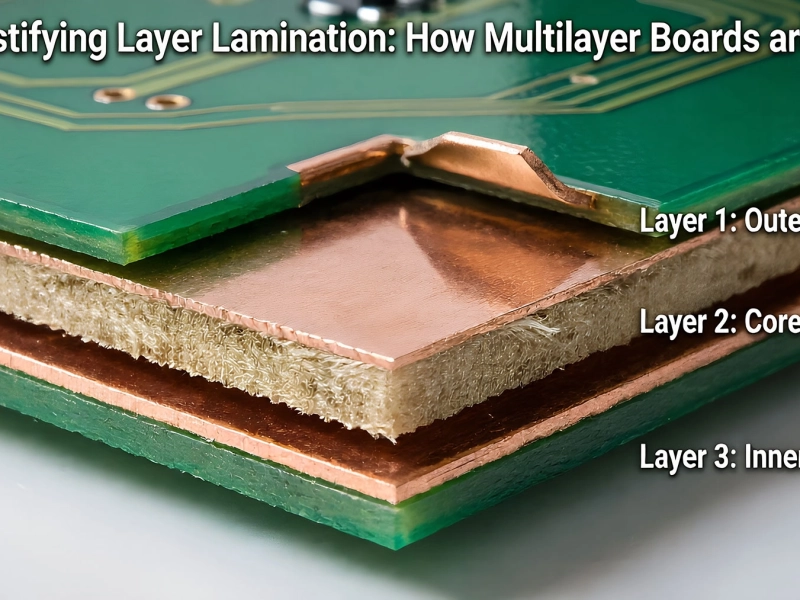
Lamination transforms the individual inner layer cores and Prepreg sheets into a single Multilayer Board.
The inner layer cores, prepreg sheets, and outer layer copper foils are stacked in the correct sequence on a lamination tooling pin fixture. The stack is placed in a lamination press between heated platens. Under controlled temperature (typically 180-190°C for standard FR-4) and pressure (typically 300-400 PSI), the prepreg resin melts and flows, bonding the layers together. After a controlled cure cycle, the press cools, and the laminated panel is removed.
Accurate layer-to-layer registration is critical. The inner layers have tooling holes that align with pins in the lamination fixture. Any misregistration at this stage causes shifted layer alignment in the finished board—vias may break out of pads, and impedance may deviate from the target. Modern fabricators use optical registration systems that align inner layers to targets etched into the copper, achieving registration accuracy of ±25-50 µm depending on layer count and board size.
After lamination, the panel is drilled to create all through-holes: component holes, via holes, and tooling holes.
A CNC drill machine loads the panel on its table, references the tooling holes or fiducial marks for alignment, and drills each hole at the coordinates specified by your Excellon drill file. Modern drill machines have multiple spindle heads that can drill several panels simultaneously, and they automatically change drill bits to match the different hole sizes in the design.
Drill speed (spindle RPM) and feed rate (how fast the bit descends) must be optimized for each hole size and the board's total thickness. Too fast a feed rate causes drill breakage and rough hole walls; too slow creates excessive heat that degrades the laminate around the hole (delamination or smear). High-aspect-ratio holes (deep, narrow holes) are the most challenging—aspect ratios above 8:1 require special drill parameters and are more prone to defects.
After drilling, the hole walls are bare fiberglass and epoxy—non-conductive. Copper plating creates the electrical connections between layers through the holes.
The panel first goes through a series of chemical cleaning and etchback steps that prepare the hole walls for plating and remove any drill smear (melted epoxy that can block the copper-to-copper interface at inner layer pads). Then the panel enters an electroless copper plating bath that deposits a thin (0.5-1 µm) layer of copper over the entire panel surface, including the hole walls. This thin electroless layer makes the entire panel electrically conductive.
Next, the panel is electroplated—connected as the cathode in a copper sulfate plating bath where additional copper is deposited under electrical current. The plating builds up copper on the hole walls and on the outer layer traces, typically adding 20-25 µm of copper. The plating thickness in the holes must meet IPC-6012 requirements for the board class—Class 2 requires minimum 20 µm average plating in the hole, Class 3 requires 25 µm.
For multilayer boards, removing drill smear from the inner layer connections is critical. If smear blocks the copper pad at the inner layer interconnect, the plated hole will have a poor or open connection to that layer. Plasma desmear (using reactive ionized gas to etch away organic material) is the most common method, followed by etchback—intentionally removing a small amount of laminate to expose more of the inner layer copper pad, creating a reliable three-point contact between the plated copper and the inner layer pad.
With the plated-through holes established, the outer layer circuit patterns are created using the same photoresist imaging and Etching Process used for inner layers—but with an important difference.
There are two approaches to creating the outer layer pattern:
For most designs, pattern plating is preferred because it allows fine-line etching on the outer layers while still building up sufficient plating in the holes.
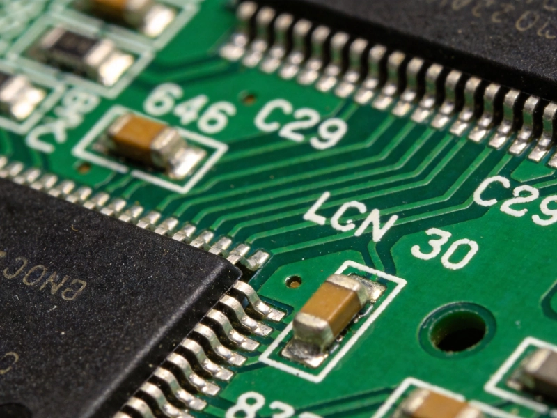
Solder Mask (solder resist) is the colored coating—most often green—that covers the board surface except where components are soldered. It prevents solder from bridging between closely spaced pads during assembly and protects the copper traces from oxidation and environmental damage.
The most common Solder Mask process uses liquid photoimageable solder mask (LPI). The board is cleaned, then the liquid solder mask is applied by screen printing or spray coating, covering the entire surface. The coating is pre-cured (tacked) to remove solvents, then exposed to UV light through a phototool or by LDI. The UV polymerizes the solder mask in the areas that should remain on the board; the unexposed areas (over the pads where soldering will occur) remain soluble. After development, the unexposed solder mask is washed away, exposing the pads. Finally, the remaining solder mask is fully cured at elevated temperature.
Green solder mask is the standard because it provides the best resolution for fine-pitch pad openings and the best contrast for visual inspection. Other colors (red, blue, black, yellow, white) are available but may have slightly lower resolution or different inspection characteristics. Solder mask thickness is typically 10-30 µm over bare copper and thinner over trace edges due to surface tension during application.
The Silkscreen or legend layer prints reference designators (R1, C2, U3), component outlines, polarity indicators, test point labels, and other information on the board surface to aid assembly and debugging.
Silkscreen ink is applied through a fine mesh screen that has the legend pattern imaged onto it—similar to traditional T-shirt screen printing, but with much finer detail. After printing, the ink is cured at elevated temperature. Alternatively, some fabricators use inkjet printers that deposit the legend directly without a screen, offering faster setup and better resolution for fine text.
The exposed copper pads—where the solder mask is not covering—must be protected from oxidation before assembly. The surface finish serves two purposes: it prevents the copper from oxidizing during storage, and it provides a solderable surface for component assembly.
Before shipping, every board is electrically tested to verify that the circuit matches the design data—no opens, no shorts.
For production quantities, a dedicated test fixture (bed of nails) is fabricated that contacts every net on the board simultaneously. The tester measures continuity (each net is connected end-to-end) and isolation (each net is isolated from every other net to a specified resistance threshold, typically 1-10 MΩ). For prototypes and small quantities, Flying Probe testers—programmable machines that move probe tips to each test point sequentially—avoid the cost of building a fixture.
Electrical Testing catches open circuits and short circuits—hard faults. It does not verify that traces are the correct width, that impedances are within tolerance, or that the dielectric thickness is correct. These are verified by other means: impedance test coupons (test traces on the production panel that are measured by TDR), cross-section analysis (cutting a sample and measuring layer thicknesses and plating under a microscope), and visual inspection.
The last steps ensure the boards meet all quality requirements and arrive at your facility in good condition.
Boards undergo a final visual inspection per IPC-A-600 (the acceptability standard for bare boards). Inspectors check for solder mask coverage, silkscreen legibility, surface finish quality, hole plating (on sample cross-sections for production runs), and dimensional compliance. Boards that pass are counted, packaged in moisture-barrier bags with desiccant for storage-sensitive surface finishes, and shipped.
For production orders, the fabricator provides a package of quality documentation including first article inspection reports, cross-section micrographs, impedance test results, electrical test reports, and material certifications (C of C). This documentation provides traceability and evidence that the boards were fabricated to specification.
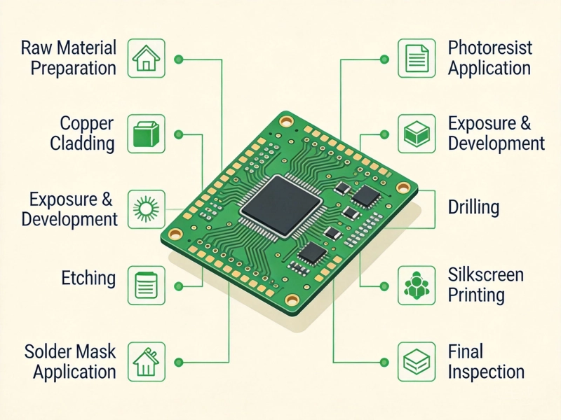
Looking at the complete flow, the manufacturing process transforms your digital design data into a physical board through a sequence of additive and subtractive operations:
Each step depends on the accuracy of the preceding steps. Registration errors in imaging propagate to etching, which propagates to drilling alignment, which affects plating quality. This cascading dependency is why process control at every stage—not just inspection at the end—is essential for high-yield manufacturing.
Every decision you make as a designer has manufacturing implications. Understanding these implications helps you design boards that are not just electrically correct but also manufacturable with high yield and reasonable cost.
The Pcb Manufacturing process is a sophisticated sequence of chemical, mechanical, and optical operations that transform raw copper-clad laminate into the precise, multilayer circuit boards that power modern electronics. Each step—from imaging through etching, lamination, drilling, plating, solder mask, and surface finish—must be executed with tight process control because errors at any stage propagate through all subsequent steps.
As a designer, understanding this process flow is not academic—it is practical knowledge that directly impacts your boards' manufacturability, cost, and yield. Design decisions that align with the capabilities and limitations of each manufacturing step result in boards that are fabricated faster, with fewer defects, and at lower cost. Decisions that ignore manufacturing reality—arbitrary trace widths, excessive unique drill sizes, unbalanced stackups—add cost and risk without adding performance.
The best designers work with their fabricators as partners, not just as vendors. Early engagement on stackup design, DFM reviews before tape-out, and clear specifications on the fabrication drawing all contribute to a smooth manufacturing flow and a successful first build. When you understand how your PCB is made, you design boards that the process can reliably produce—and that makes everyone's job easier.
Ready to discuss your Pcb Design with a manufacturer who speaks your language?Contact our engineering team for a Dfm Review, stackup consultation, or manufacturing capability discussion before your next tape-out.

E-Commerce vs. Traditional Sales: How Buying PCB Services Has ChangedJuly/25/2026
Solder Mask and Silkscreen: More Than Just Aesthetics in the PCB ProcessJuly/20/2026
A Step-by-Step Walkthrough of the PCB Fabrication ProcessMay/21/2026
Is PCB Fabrication in China Still the Most Cost-Effective Option? A 2026 AnalysisJuly/27/2026
Understanding Copper Plating: Ensuring Connectivity and Durability in PCBsJuly/09/2026

The Chemistry of PCB Cleaning: Why Ionic Contamination MattersSeptember/04/2026

Surface Preparation: The Critical Steps Before Component AssemblySeptember/16/2026
Demystifying Layer Lamination: How Multilayer Boards are BuiltJune/05/2026