In high-speed digital and RF design, Controlled Impedance is not a nice-to-have—it is a hard requirement. A 100 Ω differential pair that drifts to 112 Ω reflects enough signal energy to close the eye diagram on a 10 Gbps link. A 50 Ω RF trace that shifts to 54 Ω creates a 4 % VSWR mismatch that degrades radar sensitivity. The difference between a board that works and one that does not often comes down to whether the Pcb Manufacturer can hold impedance within ±5 % or ±7 % across every trace, on every panel, on every lot, over time.
Yet impedance tolerance is one of the most misunderstood specifications in PCB procurement. Many buyers assume that specifying "100 Ω ±10 %" on a drawing guarantees that outcome. In reality, hitting that tolerance requires the fabricator to control a chain of interdependent variables—dielectric thickness, copper weight, etch factor, line width, Prepreg resin content, and lamination pressure—each with its own variability. The manufacturer's ability to manage that chain is what separates a reliable impedance supplier from one who occasionally passes on first article but drifts out of spec in production.

The Physics of Impedance: What the Manufacturer Must Control
The characteristic impedance of a PCB trace depends on its geometry and the electrical properties of the surrounding dielectric. For a microstrip trace on an outer layer:
Z₀ ≈ (87 / √(εr + 1.41)) × ln(5.98h / (0.8w + t))
Where w is trace width, h is dielectric height to the reference plane, t is copper thickness, and εr is the Dielectric Constant. For stripline traces on inner layers, the formula is different but the dependencies are the same: trace width, dielectric thickness, copper thickness, and Dielectric Constant. A manufacturer who cannot control these four variables within tight limits cannot hold impedance—no matter how precisely they measure it.
Trace Width and the Etch Factor
Trace width is the single largest contributor to impedance error. A 4.5 mil trace that etches to 4.2 mils (a 0.3 mil reduction) shifts 100 Ω differential impedance by roughly 3–4 Ω. The etch factor—the ratio of top-width reduction to copper thickness—varies with copper weight, etchant chemistry, and equipment calibration. Key manufacturing controls include:
- CAM etch compensation. The fabricator's CAM department must widen traces in Gerber data by the expected etch-back amount before generating film or direct-imaging files. For 1 oz copper, typical compensation is 0.5–1.0 mil per side; for ½ oz, 0.3–0.5 mil per side.
- Etch uniformity across the panel. Spray-etch chambers deliver slightly different etch rates at the panel center versus the edges. Well-controlled lines use conveyorized spray systems with rotating nozzles and periodic etch-rate coupons to verify uniformity.
- Feedback from measurement. The most capable fabricators measure finished trace widths on first-article panels and feed the data back to adjust compensation for subsequent runs.
Dielectric Thickness
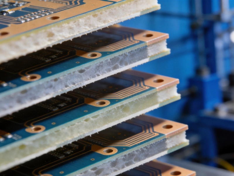
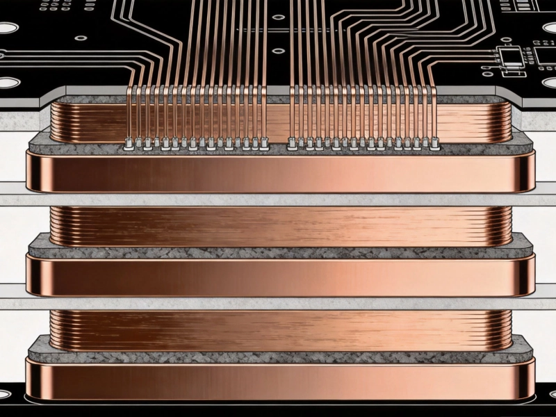
The dielectric height between the trace and its reference plane is the second most sensitive parameter. A 3.5 mil Prepreg that compresses to 3.2 mil during lamination shifts 50 Ω microstrip impedance by 2–3 Ω. Sources of variability include:
- Prepreg resin content and flow. Higher resin content means more flow during lamination, reducing final thickness. The fabricator must match the prepreg style (106, 1080, 2116, 7628) and resin content to the target thickness with <5 % tolerance.
- Lamination pressure and cycle. Over-pressing squeezes resin out of the prepreg, thinning the dielectric. Under-pressing leaves voids and inconsistent thickness. Multi-opening presses (stacking several laminations in one press cycle) can produce different thicknesses at different positions in the stack.
- Copper fill ratio. Inner-layer copper coverage affects how much resin flows to fill gaps versus remaining between planes. A layer with 60 % copper fill behaves differently from one with 20 % fill. The fabricator must account for this when selecting prepreg thickness.
Dielectric Constant (Dk) Consistency
Dk appears under the square root in the impedance equation, making it less sensitive than width or height—but still significant. A 0.1 shift in Dk (e.g., from 4.2 to 4.3) changes 50 Ω microstrip by about 0.5 Ω. The real risk is Dk variation between lots of laminate. FR-4 Dk at 1 GHz can vary ±0.2 between manufacturers and ±0.05 between lots from the same manufacturer. For tight impedance (±5 %), the fabricator must:
- Source laminate from a single qualified supplier for the duration of a production program.
- Verify Dk on incoming material using a test method (berkovich cavity, stripline resonator, or TDR-based extraction) rather than relying solely on the datasheet value.
- Track lot-to-lot Dk drift over time and adjust trace widths if necessary—known as "Dk-adjusted compensation."
Copper Thickness
Copper thickness affects impedance primarily through its influence on etch geometry and, to a lesser degree, through the t term in the impedance formula. Plated-through-hole copper (typically 20–25 µm) adds to the base copper weight on outer layers, making outer-layer impedance harder to predict than inner-layer impedance. The best fabricators specify copper thickness with ±2 µm tolerance and verify it with cross-section measurement on first articles.
Impedance Test Coupons: The Manufacturer's Report Card
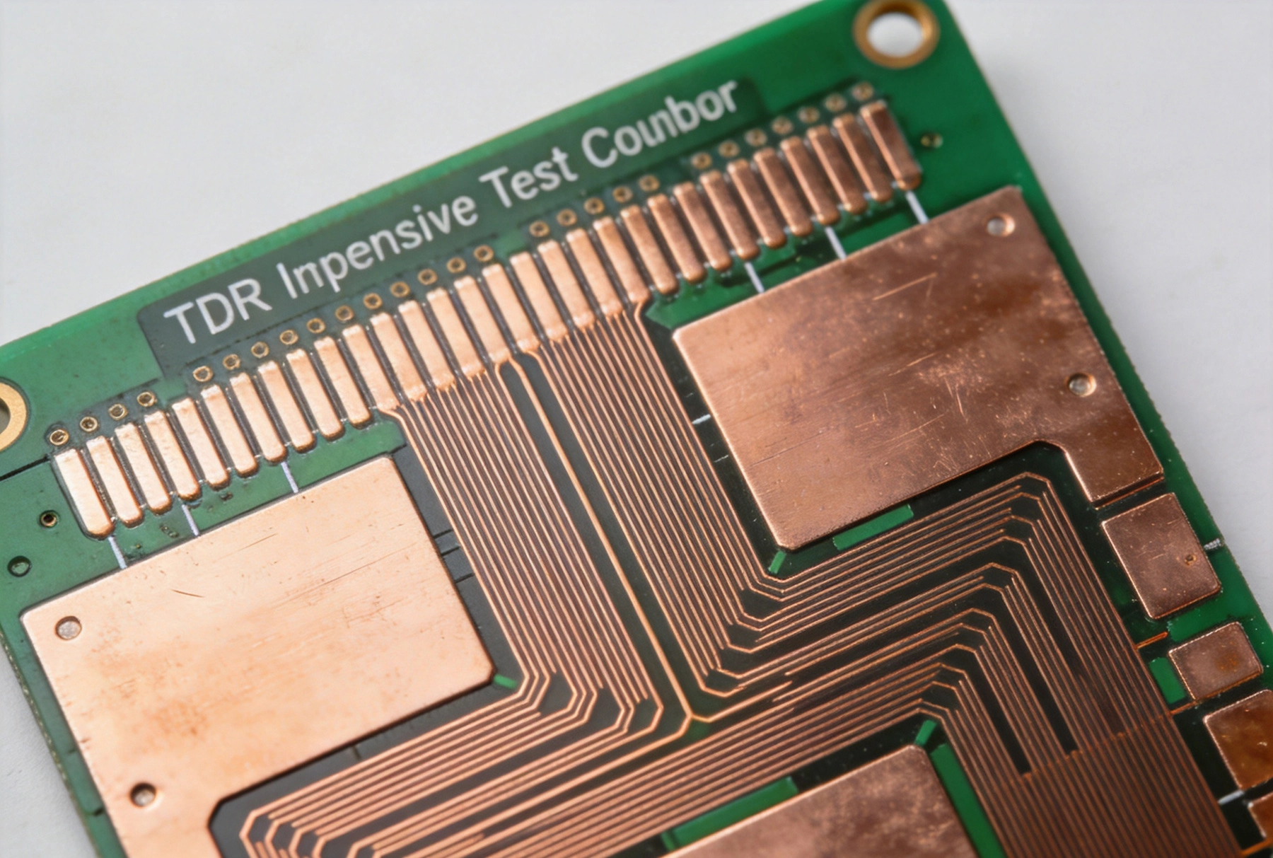
An impedance test coupon is a small PCB section—either on the production panel or a separate test panel—containing traces of each impedance type and value used in the design. The coupon replicates the exact stack-up, materials, and processing of the production board, giving the TDR a controlled geometry to measure. Evaluating a manufacturer's coupon design reveals a lot about their competence:
Coupon Architecture
- Trace length. Coupons must be long enough for the TDR to reach a stable impedance reading—at least 50 mm for single-ended traces and 75 mm for differential pairs. Short coupons reflect from the far end before the TDR settles, giving inaccurate readings.
- Launch structure. The transition from the SMA or SMP connector to the trace must be well-matched. A poor launch (wide pad, long stub, or impedance mismatch at the connector) creates artifacts in the TDR waveform that obscure the true line impedance. Look for manufacturers who use optimized coaxial launches with back-drilled or blind via transitions.
- Trace variety. The coupon should include every impedance value and trace geometry in the design: single-ended 50 Ω, differential 100 Ω, coplanar waveguide, and any specialty structures. A manufacturer who only tests the easiest geometry may be hiding problems with the harder ones.
- Reference plane continuity. The ground reference for each test trace must be solid and uninterrupted. Split planes or missing ground vias on the coupon will produce readings that do not match the production board.
What the TDR Trace Tells You
A TDR (Time-Domain Reflectometer) launches a fast step edge into the trace and measures the reflected voltage as a function of time. The reflected voltage at any point is proportional to the local impedance deviation from the reference impedance (usually 50 Ω). A skilled operator can read far more from the TDR waveform than just "pass or fail":
- Flat section = stable impedance along the trace. The length and flatness of this section indicate how uniform the manufacturing process is.
- Positive bump at the launch = impedance higher than target at the connector transition—usually an overly wide launch pad or insufficient ground clearance.
- Negative dip mid-trace = impedance lower than target—typically a local trace widening (under-etch) or dielectric thinning (resin pool).
- Gradual slope along the trace = systematic impedance drift, often caused by across-panel etch non-uniformity or prepreg thickness variation.
- Ripple or oscillation = periodic impedance variation, sometimes caused by weave pattern in the glass cloth (especially with 7628 glass style at high frequencies).
A manufacturer who only reports "pass" without showing the TDR waveform may be masking marginal performance. Request the actual TDR plots—both for first article and periodic production samples.
Statistical Process Control: Beyond First Article
First-article impedance testing confirms that a particular panel meets spec. It says nothing about the next panel, the next lot, or next year's production. A manufacturer's long-term impedance capability is measured through statistical process control (SPC):
Process Capability Indices (Cp and Cpk)
- Cp = (USL − LSL) / (6σ), where USL and LSL are the upper and lower specification limits and σ is the standard deviation of the measured impedance across many lots. Cp ≥ 1.33 means the process spread fits within the tolerance band with margin—this is the minimum for automotive and telecom applications.
- Cpk = min[(μ − LSL) / 3σ, (USL − μ) / 3σ], where μ is the process mean. Cpk accounts for how centered the process is within the spec limits. A process can have Cp = 2.0 but Cpk = 0.5 if the mean is shifted far from the target—high precision but poor accuracy.
Ask potential manufacturers for their Cp and Cpk data on Controlled Impedance. A fabricator who cannot provide this data has not done the statistical work to understand their own process capability. One who can show Cpk ≥ 1.33 over 50+ lots is a partner you can trust.
Control Charts and Trend Monitoring
Even with Cpk ≥ 1.33, process drift happens. Tooling wears, etchant chemistry changes, and laminate lots vary. SPC control charts (X-bar and R charts) track impedance measurements over time and flag out-of-control conditions before they produce out-of-spec boards. The key question for a manufacturer: Do you actively monitor impedance on control charts and adjust the process proactively, or do you only test at final inspection?
Tolerance Classes: What ±5 % Really Means
Impedance tolerances fall into three practical classes:
- ±10 % — Adequate for most single-ended signals below 1 GHz and differential pairs below 3 Gbps. Relatively easy to achieve; most competent fabricators can hold this with standard process controls.
- ±7 % — Required for 5–8 Gbps SerDes links (PCIe Gen 2/3, USB 3.0, SATA III) and most RF applications up to 6 GHz. Demands good etch compensation, Dk verification, and consistent lamination. Not all fabricators can hold this reliably in volume.
- ±5 % — Needed for 10+ Gbps links (PCIe Gen 4/5, 100G Ethernet), 77 GHz automotive radar, and sensitive RF front-ends. Requires tight control of all four impedance variables simultaneously, plus SPC monitoring and Dk-adjusted compensation. Only the top tier of fabricators can achieve this consistently.
The cost difference between tolerance classes is real but often overstated. Moving from ±10 % to ±7 % typically adds 5–10 % to fabrication cost (tighter process controls, more frequent measurements). Moving from ±7 % to ±5 % can add 15–25 % (premium materials, Dk lot verification, etch-feedback loops, and smaller panel sizes for better uniformity). The cost is justified when the alternative is a board that fails high-speed compliance testing.
Evaluating a Manufacturer: A Practical Checklist
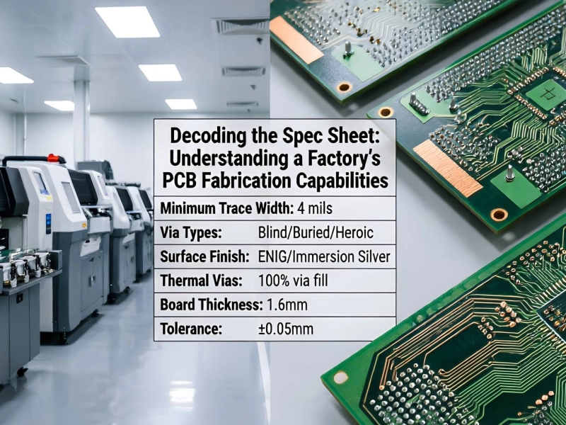
When selecting a PCB fabricator for a controlled-impedance design, go beyond the marketing claims and evaluate their actual process capabilities:
Pre-Production Evaluation
- Impedance modeling capability. Does the fabricator have their own impedance solver (Polar Si8000, Cadence LineSim, or equivalent) and use it to verify your stack-up before committing to production? A fabricator who just builds to your Gerber Files without independent verification will miss errors.
- Stack-up consultation. Will they suggest alternative stack-ups or materials that improve Impedance Control? A good fabricator pushes back on unrealistic specifications (e.g., 100 Ω ±5 % on 1080 prepreg with high Dk variance) and offers solutions.
- Coupon design review. Ask to see their standard coupon layout. Verify trace length, launch quality, and trace variety against your design requirements.
- Material sourcing. Which laminate and prepreg suppliers do they use? Do they single-source for a given program? Can they provide Dk lot certificates?
Production Capability
- Etch compensation process. Is etch compensation applied in CAM or manually? Is it adjusted per copper weight and per production lot based on measured results?
- Lamination control. Do they use multiple low-pressure press cycles or single high-pressure cycles? Do they measure post-lamination thickness on every panel?
- TDR equipment and calibration. What TDR instrument do they use (Tektronix, LeCroy, Keysight)? How often is it calibrated? Do they measure at one frequency or multiple?
- SPC data. Can they provide Cp/Cpk data for impedance on similar stack-ups to yours? How many lots does the data span?
- Cross-section capability. Do they perform cross-sections on first-article panels to verify dielectric thickness, copper thickness, and trace width—confirming the physical dimensions that determine impedance?
Ongoing Quality Assurance
- Lot-by-lot impedance testing. Is every production lot tested, or only first article? The minimum acceptable frequency is 100 % for first article and every Nth lot thereafter (N determined by Cpk; typical N = 5–10 for Cpk > 1.33).
- Trace-width verification. Do they measure finished trace widths on production panels (not just coupons) to catch etch drift?
- Material change notification. Will they notify you and re-qualify if they change laminate supplier, prepreg style, or copper foil source?
Common Pitfalls in Impedance Specification
- Specifying impedance without specifying the stack-up. Impedance is a system property, not a trace property. Two traces with identical width can have different impedances if the stack-up is different. Always specify the complete stack-up (layer order, materials, thicknesses, copper weights) alongside the impedance requirement.
- Using the Dk from the datasheet at 1 MHz for a 5 GHz design. Dk decreases with frequency for most laminate materials—by 3–5 % between 1 MHz and 5 GHz for standard FR-4. Always use the Dk at the relevant frequency, or better yet, use the manufacturer's measured Dk at the frequency of interest.
- Ignoring glass-weave effect. The glass-fiber pattern in woven laminates creates local Dk variation that causes impedance modulation along the trace. At 10+ Gbps, this "weave-induced skew" can be the dominant source of differential-to-common-mode conversion. Mitigation includes specifying rotated glass (0°/45°), spread-glass prepreg, or non-woven laminates.
- Assuming inner and outer layers have the same tolerance. Outer-layer impedance depends on plated copper thickness, which is more variable than base copper. Inner-layer impedance is typically more repeatable. Specify separate tolerances if the design allows it.
- Not accounting for Solder Mask. Solder Mask on outer-layer microstrip traces effectively increases the local Dk, lowering impedance by 1–3 Ω depending on mask thickness and Dk. The fabricator's impedance model must include solder mask; if yours does not, the built board will read low.
Case Study: Chasing ±5 % on a 100 Ω Differential Pair
Consider a 12-layer, 3.5 mm thick board with 100 Ω ±5 % differential pairs running PCIe Gen 4 at 16 GT/s. The target is 100 Ω; the tolerance band is 95–105 Ω. Here is how a top-tier manufacturer approaches the challenge:
- Stack-up design. Use Megtron 6 or I-Tera MT40 laminate for stable Dk. Select 1080 spread-glass prepreg between the signal layer and its reference plane to minimize weave effect. Target 3.7 mil dielectric height with ±0.2 mil tolerance.
- Trace width calculation. Using a 2D field solver (not empirical formula), calculate the trace width for the target Dk at 8 GHz (the Nyquist frequency of 16 GT/s). Apply etch compensation of 0.6 mil per side for ½ oz copper.
- Dk verification. Measure Dk of the incoming laminate lot using a stripline resonator test at 8 GHz. If the measured Dk differs from the target by more than 0.03, adjust trace width in CAM before imaging.
- Lamination control. Use a single-opening press with measured pressure uniformity across the platen. Measure post-lamination dielectric thickness on the coupon with cross-section.
- Etch feedback. After first-article, measure finished trace width on the coupon with optical measurement. If the trace is 0.1 mil wider than target, reduce CAM compensation by 0.1 mil for the next lot.
- SPC monitoring. Plot coupon impedance on X-bar and R charts. If Cpk drops below 1.33, investigate root cause before shipping more boards.
This loop—model, measure, adjust, monitor—is what separates manufacturers who can hit ±5 % from those who can only hope to. It requires investment in equipment (field solver, Dk test fixtures, cross-section lab), process engineering discipline, and a culture of continuous improvement rather than "build and ship."
Conclusion
Controlled impedance is a manufacturing capability, not a line item on a specification sheet. The tolerance you write on your drawing is only as good as the fabricator's ability to control the four variables that determine impedance: trace width, dielectric thickness, copper thickness, and dielectric constant. A manufacturer who controls these variables with SPC, adjusts compensation based on measurement data, and verifies every lot with well-designed impedance coupons is a partner who will deliver boards that meet spec consistently. One who relies on fixed CAM compensation and first-article-only testing will eventually deliver boards that drift out of tolerance—usually on the lot you cannot afford to scrap.
When evaluating PCB fabricators for controlled-impedance work, ask the hard questions: show me your Cp/Cpk data, show me your coupon design, show me your TDR waveforms, and tell me how you adjust when the process drifts. The answers—or the lack of them—will tell you everything you need to know.
For controlled-impedance PCB Fabrication with demonstrated ±5 % capability, SPC-monitored production, and full impedance traceability, contact our team to discuss your stack-up and tolerance requirements.
FAQ
What is a good impedance tolerance for high-speed PCBs?
For signals below 3 Gbps, ±10 % is generally adequate. For 5–8 Gbps links, ±7 % is recommended. For 10+ Gbps SerDes and millimeter-wave RF, ±5 % is the target. Tighter tolerances require more capable fabricators and higher fabrication cost.
How is PCB impedance measured?
Impedance is measured using Time-Domain Reflectometry (TDR). The TDR launches a fast voltage step into the trace and measures reflected energy. The reflection coefficient at any point reveals the local impedance deviation from the TDR's reference impedance (typically 50 Ω).
What is an impedance test coupon?
A test coupon is a PCB section on the production panel that contains traces matching each impedance type and value in the design. It uses the same stack-up, materials, and processing as the production board, providing a controlled geometry for TDR measurement without probing the actual board.
Why does impedance drift between production lots?
Impedance depends on trace width, dielectric thickness, copper thickness, and Dk. Each of these varies with etchant condition, lamination pressure, copper plating consistency, and laminate lot characteristics. Without active process monitoring and compensation, these small variations accumulate across lots.
What does Cpk ≥ 1.33 mean for impedance?
Cpk (Process Capability Index) measures how well a manufacturing process stays within specification limits, accounting for both process spread and centering. Cpk ≥ 1.33 means the process is capable of producing less than 63 defects per million opportunities—widely accepted as the minimum for automotive and telecom quality requirements.