Open Nav

The era when standard PCB designs could satisfy most product requirements has passed. As technology advances across industries from artificial intelligence to electric vehicles, the demands placed on electronic hardware have grown far beyond what generic solutions can address. Product engineers and hardware designers increasingly find that off-the-shelf PCBs constrain their ability to achieve the performance, integration, and reliability their applications require.
This shift reflects broader trends in Electronics Miniaturization, functional complexity, and application-specific requirements. Understanding why Custom Pcb solutions have become essential helps product teams make better decisions about Hardware Development strategies and manufacturing partnerships.
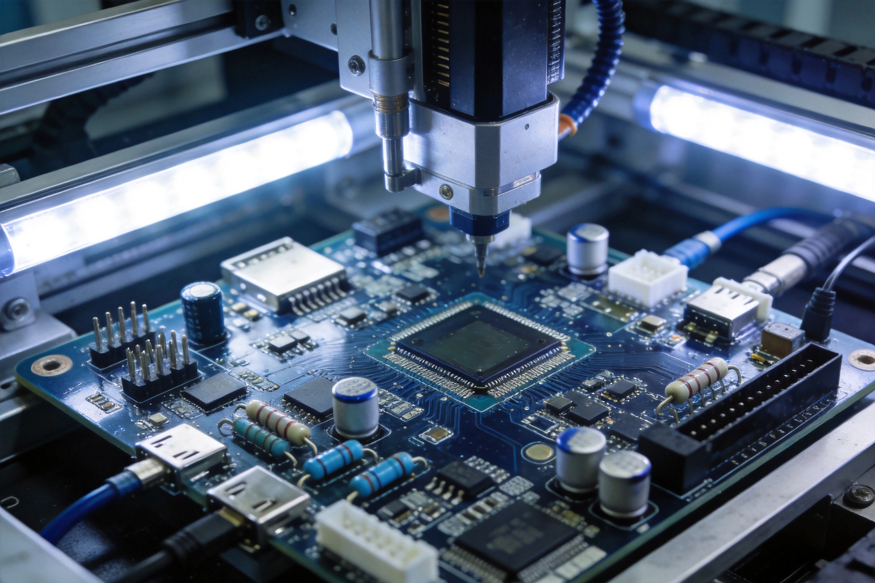
Early consumer electronics and industrial equipment used relatively simple circuits that could be implemented with standard board configurations. Designers selected from available board sizes, layer counts, and material options, adapting their circuits to fit generic constraints. This approach worked when electronic systems performed straightforward functions and competed primarily on cost rather than performance differentiation.
Modern products demand far more sophisticated implementations. A smartphone contains radios, sensors, power management, application processors, memory, and display interfaces all operating simultaneously while fitting in a pocket-sized enclosure. An electric vehicle manages battery systems, motor drives, safety systems, and connectivity functions that interact in complex ways. These requirements cannot be met with generic PCB solutions.
Product marketability often depends on size and weight reduction. Consumers expect smaller, lighter devices without sacrificing functionality. Industrial equipment manufacturers seek compact enclosures that reduce floor space and improve aesthetics. Medical device developers need implantable electronics small enough for minimally invasive procedures.
Miniaturization drives several PCB requirements that standard solutions cannot address. High-density Interconnect (HDI) technologies enable more routing in less space. Custom stack-ups optimize Signal Integrity while minimizing board area. Embedded components place passive devices within the board structure rather than占用 surface area. These capabilities require close coordination between design and manufacturing that generic board suppliers cannot provide.
Edge computing applications process data locally rather than transmitting everything to cloud servers. This approach reduces latency, improves reliability in connectivity-limited environments, and addresses data privacy concerns. However, edge processors often perform machine learning inference, requiring high-speed memory interfaces and careful Signal Integrity management.
High-speed digital design demands Impedance Control, differential pair routing, and layer stack-ups optimized for signal integrity. Generic PCBs may offer some Controlled Impedance options, but rarely with the precision or consistency that advanced processors require. Custom solutions enable exact specification of impedance tolerances, via stub control, and crosstalk management that high-speed signals demand.
AI accelerators and machine learning processors represent some of the most demanding PCB applications currently in production. These chips require high-bandwidth memory interfaces operating at multiple gigabytes per second, extensive power delivery networks with hundreds of amps at low voltages, and sophisticated Thermal Management to handle tens of watts in compact packages.
Standard PCB approaches cannot meet these requirements. Memory interfaces need precise timing tolerances that require custom stack-up design and manufacturing control. Power delivery for AI chips requires specialized decoupling networks, island avoidance, and current return path planning that generic designs ignore. Thermal Management may demand metal core substrates, embedded heat spreaders, or hybrid constructions that standard processes do not support.
IoT products span a wide range from simple sensors to complex gateways, but all share common pressures toward smaller size, lower cost, and extended battery life. Simple generic boards may handle basic sensor nodes, but anything beyond entry-level functionality requires custom approaches.
Wireless connectivity adds RF design requirements to PCB requirements. Wi-Fi, Bluetooth, Zigbee, LoRa, and cellular modules need careful antenna integration, ground plane design, and matching network implementation. These RF considerations interact with board geometry in ways that generic solutions cannot address. The growing demand for dual-band Wi-Fi, Bluetooth LE audio, and other advanced wireless features further complicates RF layout requirements.
Power consumption optimization in battery-powered IoT devices extends beyond chip selection to PCB-level considerations. Leakage paths, ground reference quality, and decoupling network design affect sleep currents and operational efficiency. Custom Pcb design enables optimization across all these dimensions in ways that standard solutions cannot match.
Automotive applications face unique challenges including extended temperature ranges, vibration exposure, and long product lifetime requirements. Safety-critical systems demand design practices that generic PCB suppliers do not implement by default. The shift toward electric vehicles amplifies these requirements while adding high-current power delivery challenges.
Automotive PCB requirements typically include extended temperature range materials, enhanced plating thickness for durability, and documentation supporting functional safety analysis. Custom design enables selection of appropriate materials and construction for specific automotive environments, from under-hood temperatures to interior comfort systems.
Advanced driver assistance systems (ADAS) combine high-speed processing with sensor interfaces including cameras, radar, and lidar. These systems require boards that support both high-speed data interfaces and precise timing for safety-critical sensor fusion. Generic solutions lack the control necessary for these demanding applications.
Medical devices must meet stringent regulatory requirements while often demanding miniaturization for implantable or handheld use. The combination of Size Constraints, reliability requirements, and regulatory compliance creates design challenges that standard PCBs cannot address.
Implantable medical devices push miniaturization to extreme limits while requiring exceptional reliability. These applications benefit from custom stack-ups that minimize board size, materials selected for biocompatibility and long-term stability, and construction techniques that ensure reliability over decades of operation. Custom manufacturing enables the process controls and documentation that regulatory submissions require.
Wearable medical devices balance Size Constraints with functionality requirements and battery life targets. Flexible and rigid-flex PCB constructions enable form factors that rigid boards cannot achieve. Custom design optimizes bend radius constraints, dynamic flex requirements, and integration of multiple rigid sections with flexible interconnect.
Industrial equipment operates in electrically noisy environments with electromagnetic interference, voltage transients, and thermal cycling. Pcb Design for industrial applications must address these environmental challenges while often supporting long product lifetimes and backward compatibility requirements.
Motor drives and Power Electronics within industrial equipment demand PCB constructions supporting high current flow, thermal management for power devices, and isolation between signal and power circuits. Custom design enables optimization of ground planes, thermal vias, and clearance requirements for specific power levels and voltage ratings.
Industrial communication interfaces including EtherCAT, PROFINET, and other fieldbus protocols have specific layout requirements for reliable operation in industrial environments. Signal integrity considerations for these interfaces often require custom trace geometry, termination schemes, and ground plane management that generic boards cannot provide.
Standard Pcb Services typically offer common layer counts (2, 4, 6, 8) with fixed material options. While adequate for many applications, these constraints limit Design Optimization. High-speed designs may benefit from specialized core and Prepreg sequences that generic processes do not support. RF designs may need specific dielectric constants or loss characteristics that standard materials do not provide.
Custom stack-up design enables exact specification of layer functions, material types, and thickness tolerances for specific application requirements. A high-speed digital design might specify Controlled Impedance layers with specific reference plane configurations. An RF design might use dedicated RF materials only where needed, reducing cost compared to full-board specialty materials.
Standard Pcb Services enforce generic Design Rules suitable for typical applications. These rules often include safety margins that conservative for many designs but restrictive for advanced applications. Minimum feature sizes, via dimensions, and spacing rules may prevent optimal implementations.
Custom PCB services can specify Design Rules matched to specific capabilities and application requirements. Dense digital designs benefit from tight trace and space rules that reduce board area. High-reliability designs may use expanded clearances and enhanced plating beyond standard specifications. Custom rules enable optimization for the specific balance of density, reliability, and manufacturing yield that each project requires.
Standard Pcb Materials serve general-purpose applications but may not meet specific requirements for thermal performance, high-frequency characteristics, or environmental resistance. Materials optimized for specific applications often carry significant cost premiums or require minimum order quantities that limit their use.
Custom Pcb Design enables material selection matched to application requirements. High-temperature applications benefit from elevated glass transition temperature (Tg) materials. High-frequency applications use low-loss dielectrics where signal integrity demands them. Flexible applications require Polyimide or flexible substrate materials. Each material choice affects board cost, manufacturing process, and long-term reliability in ways that require application-specific evaluation.
Custom PCB development integrates design with manufacturing process capabilities. Engineers work with manufacturers to ensure that designs are producible with acceptable yields and that manufacturing processes support design requirements. This collaboration identifies potential problems early when design changes are inexpensive rather than late in production when changes are costly.
Design For Manufacturing (Dfm) analysis for custom PCBs examines feature tolerances, panel utilization, and process capability interactions. Complex designs benefit from Dfm-driven layout adjustments that improve manufacturability without compromising performance. This optimization level is impossible with generic solutions that do not consider specific project requirements.
Custom PCB relationships often include Supply Chain support that standard procurement cannot match. Manufacturers may stock common materials and components, provide Inventory Management for long-term programs, or support last-time buys for components approaching obsolescence. These services reduce Supply Chain risk for products with extended lifecycles.
Custom relationships also enable configuration management and change control that high-reliability applications require. Documentation of material substitutions, process changes, and manufacturing location transfers supports regulatory compliance and customer quality requirements. Standard procurement lacks the traceability and control that demanding applications need.
Custom PCB development enables optimization across multiple performance dimensions simultaneously. A design might simultaneously optimize signal integrity for high-speed interfaces, thermal performance for power devices, and size reduction for enclosure constraints. These interconnected requirements cannot be balanced effectively within the constraints of standard solutions.
Performance optimization includes electrical, thermal, mechanical, and reliability considerations. Custom solutions enable trade-off analysis across these dimensions with full awareness of how changes in one area affect others. The resulting designs achieve performance levels that generic approaches cannot match.
Not every project requires custom PCB development. Simple applications, prototypes with flexible timelines, and cost-sensitive products with minimal performance requirements may be served well by standard solutions. The decision to pursue custom development should be based on clear requirements that standard solutions cannot meet.
Indicators that custom development may be necessary include performance requirements that exceed standard capabilities, size constraints requiring advanced technologies like HDI or embedded components, environmental challenges that standard materials cannot address, regulatory requirements demanding documentation and traceability, or competitive pressure for features that generic solutions cannot support.
Custom PCB development requires close collaboration between product engineers and manufacturing partners. Early engagement enables manufacturers to provide input on feasibility, identify potential problems, and suggest optimizations that improve outcomes. This collaboration works best when both parties understand project requirements and constraints.
Expect custom manufacturers to ask detailed questions about application requirements, performance targets, environmental conditions, and lifecycle expectations. These questions are not bureaucratic obstacles but essential information for developing appropriate solutions. Manufacturers who ask detailed questions demonstrate the engagement level necessary for successful custom development.
Custom Pcb Solutions typically cost more than standard alternatives due to specialized materials, additional process steps, and reduced economies of scale. However, cost comparisons should consider total cost of ownership rather than just unit price. Custom solutions may reduce other costs through improved yields, reduced rework, enhanced reliability, and extended product lifetime.
Cost optimization for custom PCBs includes design practices that reduce manufacturing complexity without compromising performance. Panel utilization, feature density, and process step minimization all affect cost. Working with manufacturers to understand cost drivers enables informed decisions about design trade-offs.
The trend toward greater integration continues, with advanced packaging technologies like embedded multi-die interconnect桥接 (EMIB), 2.5D interposers, and fan-out wafer-level packaging (FOWLP) enabling unprecedented levels of integration. These technologies blur traditional boundaries between IC packaging and Pcb Assembly, creating new design and manufacturing paradigms.
Custom PCB development increasingly intersects with these advanced packaging approaches. Designers must consider package-level integration alongside board-level design, with interactions between chip placement, substrate design, and board layout. This integration requires even closer collaboration between product teams and manufacturing partners.
The semiconductor industry shift toward chiplet architectures disaggregates traditional monolithic chips into modular die assemblies. This approach enables mixing of process technologies and facilitates yield improvement but places new demands on PCB and substrate design. High-bandwidth die-to-die interfaces, shared memory architectures, and heterogeneous integration all require board-level support.
Chiplet-based systems demand custom PCB approaches that address unique requirements for die-to-die interfaces, power delivery to multiple chips, and thermal management across heterogeneous assemblies. Standard solutions cannot address these emerging requirements.
Environmental Sustainability increasingly influences PCB design and manufacturing decisions. Material selection, energy efficiency during manufacturing, and end-of-life recyclability all factor into product environmental impact. Custom solutions can address Sustainability requirements that standard options may ignore.
Designers seeking to minimize environmental impact benefit from custom approaches that optimize material usage, enable lead-free and halogen-free constructions, and support repairability and upgradeability. These considerations interact with electrical and thermal design in ways that require holistic optimization.
Choose custom development when your application has requirements that standard PCBs cannot meet. This includes high-speed designs needing tight impedance tolerances, RF applications requiring specific dielectric properties, extreme environments demanding specialized materials, size constraints requiring HDI or embedded technologies, or regulatory requirements needing documentation and traceability.
Custom PCBs typically cost more due to specialized materials, additional process steps, and lower manufacturing volumes. However, cost differences vary widely based on complexity, quantities, and specific requirements. Evaluate total cost of ownership including manufacturing yields, rework rates, and field reliability rather than just unit price when comparing options.
Lead times vary based on complexity and manufacturer capacity. Simple custom designs may add only modest time to standard lead times. Complex designs requiring new tooling, specialized materials, or extensive qualification may require significantly longer timelines. Discuss requirements early with manufacturers to establish realistic schedules.
Look for manufacturers with experience in your application area, demonstrated capabilities matching your requirements, quality systems supporting your reliability needs, and willingness to engage early in design development. Request samples, references, and documentation of their process capabilities. The right manufacturer relationship extends beyond procurement to genuine partnership.
The transition from off-the-shelf to Custom Pcb Solutions reflects broader shifts in electronics technology. As products demand greater performance, miniaturization, and integration, standard PCB approaches become increasingly inadequate. Custom development enables the optimization necessary to meet these demanding requirements while balancing cost, reliability, and time-to-market pressures.
Product teams should evaluate their specific requirements against standard solution capabilities, engaging custom manufacturers early when gaps exist. The investment in custom PCB development often delivers returns through improved product performance, reduced manufacturing and field failure costs, and competitive differentiation that standard solutions cannot provide.
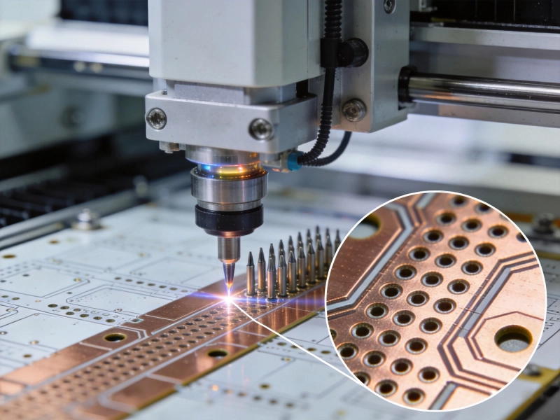
The Art of Drilling: Mechanical vs. Laser Drilling in Modern PCB ManufacturingJune/26/2026
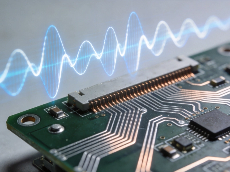
High-Frequency Materials: Assessing Capabilities for RF and Microwave PCBsJuly/23/2026
E-Commerce vs. Traditional Sales: How Buying PCB Services Has ChangedJuly/25/2026
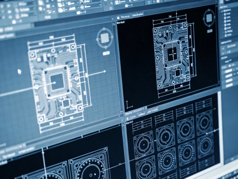
Best Practices for Preparing Files for Expedited PCB ManufacturingJuly/29/2026
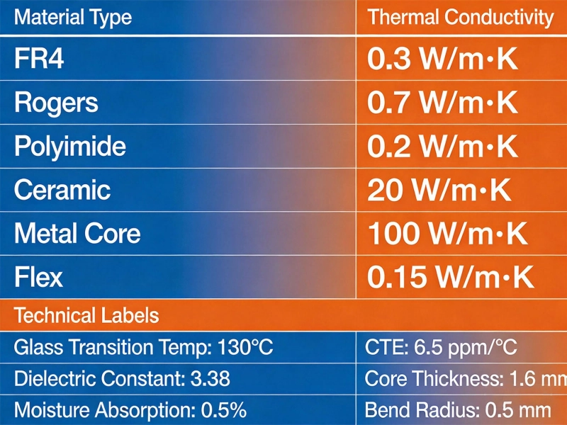
Exploring Special Materials in Custom PCB FabricationMay/21/2026

Challenges in Manufacturing High Aspect Ratio Multilayer BoardsSeptember/07/2026
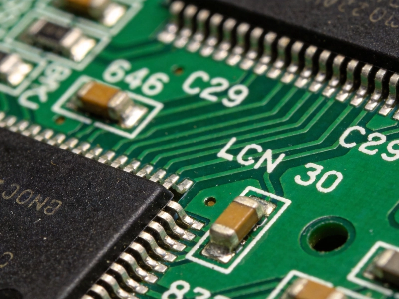
Solder Mask and Silkscreen: More Than Just Aesthetics in the PCB ProcessJuly/20/2026
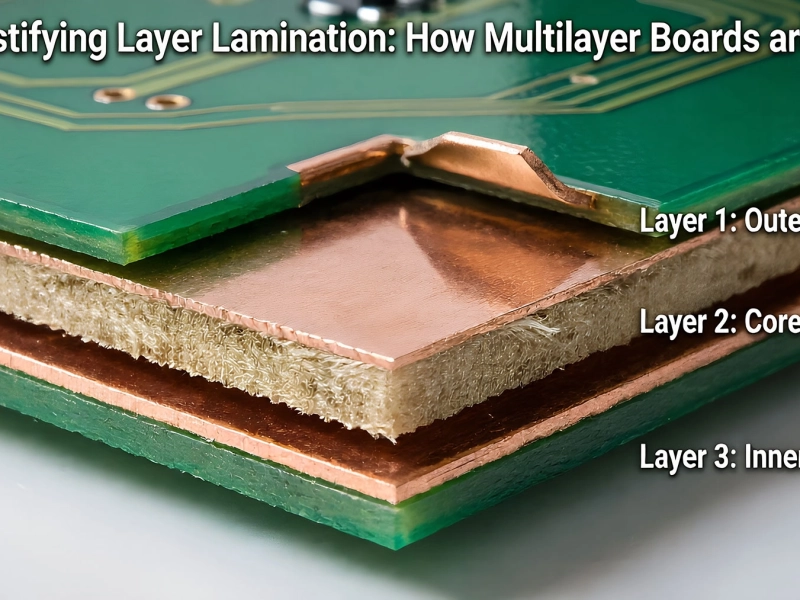
Demystifying Layer Lamination: How Multilayer Boards are BuiltJune/05/2026