Open Nav

High aspect ratio Multilayer Boards sit at the edge of what Pcb Manufacturing can reliably produce. When your design requires dozens of layers with tiny vias connecting signals deep in the stack, you enter territory where standard fabrication processes break down and specialized techniques become essential. Understanding these challenges helps you make informed decisions about your board construction and sets realistic expectations for what manufacturers can deliver.
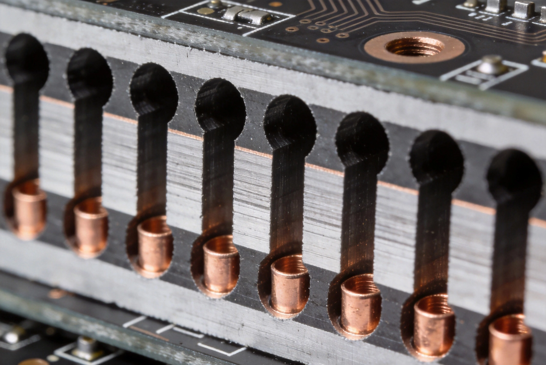
Aspect ratio describes the relationship between a via's depth and its diameter. A via that is 1.2 millimeters deep with a 0.3 millimeter drill diameter has an aspect ratio of 4:1. Standard Pcb Manufacturing comfortably handles aspect ratios up to about 8:1. Beyond that threshold, physics and chemistry conspire to create defects that are difficult or impossible to eliminate completely.
High aspect ratio Multilayer Boards combine deep via structures with complex layer stacking. A twelve-layer board with 0.15 millimeter vias creates aspect ratios approaching 10:1 or higher. Each additional layer adds depth while maintaining small diameters for routing density. The combination of depth and complexity multiplies the manufacturing difficulty.
Designers request high aspect ratio structures for several reasons. Dense routing requires small vias that occupy less board real estate. Blind and buried via designs need small diameters to fit between layers. High-layer-count boards require deeper drilling to connect the many internal layers. Each requirement pushes toward higher aspect ratios.
Drilling high aspect ratio holes strains mechanical drilling equipment to its limits. The drill bit must penetrate deeply while maintaining diameter tolerance and positional accuracy. As drill depth increases, tool deflection becomes significant. A bit that vibrates even slightly during entry creates an oversized hole at the top and an even worse profile at the bottom.
Laser Drilling offers an alternative for very small vias, particularly in HDI constructions. CO2 lasers can ablate dielectric material without the mechanical forces that cause drill wander. However, Laser Drilling cannot penetrate copper, so the target copper pad must be treated specially or the laser must be configured for specific layer stops.
PCB drill bits wear faster when penetrating multiple copper layers and thick substrates. Carbide bits maintain sharpness longer than high-speed steel but are more brittle and prone to breaking in deep holes. Some manufacturers use peck drilling cycles that retract the bit periodically to clear chips and cool the tool. This approach is slower but produces better hole quality in deep structures.
Electroplating Copper into high aspect ratio holes presents one of the most difficult challenges in PCB manufacturing. The electroplating solution carries copper ions to the hole surface, where they deposit as metal. In a deep narrow hole, ions must travel far down the hole and back out against the solution flow. The result is uneven copper distribution with thick copper at the hole entrance and thin copper deep inside.
The fundamental problem is solution depletion. As current passes through the hole, copper ions near the opening deposit first, leaving the solution entering the hole progressively starved of ions. By the time solution reaches the hole bottom, ion concentration is too low for adequate deposition. This phenomenon, called throw power limitation, becomes severe at high aspect ratios.
Manufacturers address this through several techniques. Pulse plating alternates current direction to improve ion distribution. Specialized chemistry with high throwing power salts enhances penetration depth. Agitation systems that create solution flow into holes improve ion transport. Despite these improvements, copper thickness at the hole bottom in a 10:1 aspect ratio via may be only 60-70% of the entrance thickness.
Voids are air pockets trapped inside plated via barrels during the plating process. In low aspect ratio holes, voids rise to the surface and escape naturally. In high aspect ratio structures, voids become trapped halfway down the hole where solution cannot reach them. Once the plating grows over the void, it becomes permanently enclosed.
Voids create multiple problems. They reduce the via's current-carrying capacity by eliminating copper from part of the cross-section. Thermal resistance increases in the void region, creating hot spots during operation. Mechanical strength decreases because the void removes material from the barrel. In extreme cases, thermal cycling causes the copper near voids to crack due to differential expansion.
Preventing voids requires careful process control. Reverse-pulse plating periodically dissolves thin deposited copper that can trap bubbles, then replates more uniformly. Ultrasonic agitation before plating helps release air bubbles from hole surfaces. Some manufacturers use vacuum impregnation to pull air out of holes before plating begins. Despite these measures, very high aspect ratios inevitably produce some voids that are technically acceptable under IPC guidelines.
Multilayer boards with many layers require many lamination cycles. Layer pairs are pressed together, then additional layers are added through sequential lamination or multilayer pressing. Each cycle exposes the board to temperatures above 180 degrees Celsius while pressure bonds the Prepreg sheets between copper layers.
High aspect ratio vias complicate lamination because they create channels through the board that can trap air and volatiles. Prepreg resin flows into holes during lamination, but if gas is trapped ahead of the resin front, voids form in the hole barrel. Alternatively, the resin can wick away from the hole barrel, leaving insufficient encapsulation.
Delamination risk increases when high aspect ratio vias create stress concentrations at layer interfaces. The difference in thermal expansion between copper via barrels and surrounding prepreg creates stress during cooling. In extreme cases, this stress exceeds the bond strength between layers and causes separation. High aspect ratio vias with thin plating are particularly vulnerable because the copper barrel can flex more during thermal cycles.
Aligning dozens of layers in a thick Multilayer Board strains the limits of optical registration systems. Each layer's artwork must be positioned precisely relative to the layers above and below. As boards get thicker and hole depths increase, optical focus becomes challenging. Inner layers that are millimeters below the surface may be out of focus for cameras viewing from either side.
Registration tolerance accumulates through the stack. If each layer is misregistered by 25 micrometers relative to its adjacent layers, a twelve-layer board has potential for 300 micrometers total offset between the top and bottom layers. High aspect ratio vias that must connect specific inner layers are most affected because the positional error compounds with depth.
Manufacturers use multiple strategies to improve registration. Better material handling reduces distortion during layer preparation. Automated optical inspection after each lamination step identifies problems before additional layers are added. Sequential lamination builds thick boards in stages rather than pressing everything at once, limiting registration errors to each incremental addition. These approaches add cost and time but enable reliable high-layer-count production.
Etching removes unwanted copper from the substrate to form traces and pads. In multilayer boards, the outer layers undergo etching after all inner layers are laminated. The etchant must penetrate into the board edges and around features without over-etching the fine details or under-etching the coarse power planes.
High aspect ratio boards present unique etching challenges. The board thickness means etchant diffusion to inner areas is slower than in thin boards. This can leave residual copper in areas where etchant cannot reach adequately, causing shorts between features. Alternatively, the extended etch time needed for thick boards can over-etch fine traces, making them too narrow.
Conductor profile refers to the cross-sectional shape of etched traces. Ideal traces have vertical sidewalls, but practical etching produces slightly tapered profiles. The taper angle increases with board thickness because etchant attacks the copper at the base longer than at the top. For fine-pitch components on thick boards, this profile affects solder joint reliability and clearances.
Testing continuity and isolation on high aspect ratio multilayer boards pushes the capabilities of standard test equipment. The resistance of long vias through many layers is low but measurable. Accurately measuring milliohms while accounting for probe contact resistance requires sophisticated instrumentation.
High aspect ratio vias can have subtle opens that pass basic continuity checks but fail under thermal stress or mechanical vibration. An via barrel with only 70% copper thickness at the bottom may test as connected but fail when current flows during operation. Accelerated Life Testing reveals these marginal structures that pass standard testing.
Isolation testing between adjacent nets becomes more critical as trace density increases. High aspect ratio boards often have tight spacing between features to maximize routing density. Capacitive coupling between nearby high-aspect-ratio vias can cause crosstalk at high frequencies. Vector network analyzers can measure these RF characteristics, but such testing is expensive and typically reserved for specialized applications.
X-ray Inspection is essential for verifying high aspect ratio via quality. Standard optical inspection cannot see inside via barrels, so X-ray provides the only non-destructive view of plating uniformity and void content. Manufacturers use both 2D projection X-ray and 3D computed tomography for different inspection purposes.
2D X-ray clearly shows via barrel cross-sections, revealing thin plating, voids, and cracks. Inspection technicians compare barrel images against acceptance criteria. 3D CT scanning provides complete volumetric data but is slow and expensive, making it suitable for failure analysis rather than production inspection.
Cross-sectioning destructive tests physically cut boards to expose via structures for examination. This method provides the most detailed view of plating quality, lamination bond integrity, and conductor profile. Manufacturers typically cross-section first article boards from each production lot to establish process capability. Production boards are not cross-sectioned, so first article results must represent the lot.
Designing with manufacturing limitations in mind improves first-pass success rates. Avoid requiring blind or Buried Vias on every layer. Reserve high aspect ratio connections for nets that genuinely need them. Route signals on layers that minimize drilling depth requirements.
Specify adequate annular rings around vias. High aspect ratio drilling has larger positional tolerance than shallow drilling due to drill wander and registration limitations. A pad that is barely large enough for a shallow via may have insufficient margin for a deep via. Generous annular rings accommodate drilling variation without reducing effective drill diameter below the design minimum.
Consider using parallel-leg or staggered via structures instead of straight-through vias. A pair of 6:1 aspect ratio vias is easier to plate reliably than a single 12:1 via. Staggered via configurations connect inner layers through intermediate layers rather than spanning the full board thickness in one structure.
Not all PCB manufacturers can produce high aspect ratio multilayer boards reliably. Evaluating manufacturer capabilities requires understanding their equipment, process controls, and experience base. Ask about their maximum demonstrated aspect ratio, the yield rates they achieve at various aspect ratios, and what specialized processes they use for deep hole structures.
Request capability documentation including statistical process control data for critical parameters like plating thickness uniformity, void rates, and registration accuracy. Manufacturers who invest in SPC typically have better process discipline and more consistent results. Ask for capability indices like Cpk values that quantify process capability.
Review their quality management system certification. ISO 9001 provides general quality management framework, while AS9100 and Iatf 16949 add requirements specific to aerospace and automotive applications. NADCAP certification is required for some defense and aerospace customers. These certifications indicate that the manufacturer has documented processes and audit trails.
High aspect ratio multilayer boards cost significantly more than standard constructions due to process complexity, specialized equipment, lower yields, and extended testing requirements. A twelve-layer board with 10:1 aspect ratio vias might cost three to five times more than an equivalent eight-layer board with standard aspect ratios.
Lead times also extend considerably. Deep drilling takes longer than shallow drilling. Plating cycles may require multiple steps to achieve adequate thickness. Additional inspection and testing verify quality at each stage. Production lots with high aspect ratio structures typically require four to eight weeks, compared to two to three weeks for standard multilayer boards.
These costs and lead times are justified for applications that genuinely require high aspect ratio structures. Evaluate whether your design genuinely needs this complexity or whether an alternative construction could meet your requirements at lower cost. Sometimes reducing layer count and using HDI Microvias achieves the same functionality more economically.
Advanced HDI constructions using sequential lamination and Microvia Technology offer alternatives to traditional high aspect ratio through-holes. Instead of drilling deep holes through the entire board, designers build up layers with small laser-ablated Microvias. Each Microvia spans only one or two layers, keeping aspect ratios manageable.
Any-layer HDI technology connects any layer to any other using Microvia structures without requiring through-hole drilling across the full board thickness. While more expensive per layer than standard HDI, any-layer construction eliminates the reliability concerns of deep through-holes while providing maximum routing flexibility.
Embedded passive components and substrate-like packaging represent another approach. By embedding resistors, capacitors, and even active devices within the board structure, designers reduce the layer count and via density required for complex functions. These technologies are more expensive but enable significant size reduction.
Manufacturing high aspect ratio multilayer boards tests the boundaries of standard PCB Fabrication. Drilling deep small holes stresses equipment, plating uniformity suffers in narrow structures, voids become trapped in deep barrels, and lamination creates stress concentrations that risk delamination.
The fundamental challenges involve transport phenomena. Electroplating solution cannot reach deep into narrow holes effectively. Etchant and developer must diffuse through thick boards. Gases and volatiles cannot escape from deep structures during lamination. Each step of manufacturing involves chemistry and physics that behave differently at depth.
Designing for manufacturability helps. Use the lowest aspect ratio that meets your routing needs. Specify generous annular rings. Reserve high aspect ratio structures for critical nets. Consider alternatives like staggered vias or HDI microvia constructions that avoid deep drilling entirely.
Working with experienced manufacturers who understand these challenges improves outcomes. Provide clear documentation of your requirements, ask about their process controls, and verify capability with first article inspection. Budget appropriately for the higher cost and longer lead times that these complex structures require.
By understanding why high aspect ratio multilayer boards are difficult to manufacture, you can make informed trade-offs between design density and manufacturing feasibility.
Understanding the PCBA Workflow: From Gerber Files to Finished BoardJune/16/2026

The Importance of BOM Accuracy in the PCB Assembly ProcessJuly/13/2026

The Benefits of Combining PCB Fabrication and AssemblyMay/22/2026
SMT vs THT PCB Assembly in China: Which Technology is Right for Your Project?June/10/2026
PCB Fabrication and Assembly: A Step-by-Step Guide for BeginnersOctober/15/2026

Inspection Standards: IPC-A-610 and What it Means for Your Assembled BoardsAugust/03/2026

Turnkey Assembly: How to Hand Off Your Project and Get Finished ProductsJuly/22/2026

Prototyping vs. Production Assembly: Different Approaches for Different StagesSeptember/08/2026