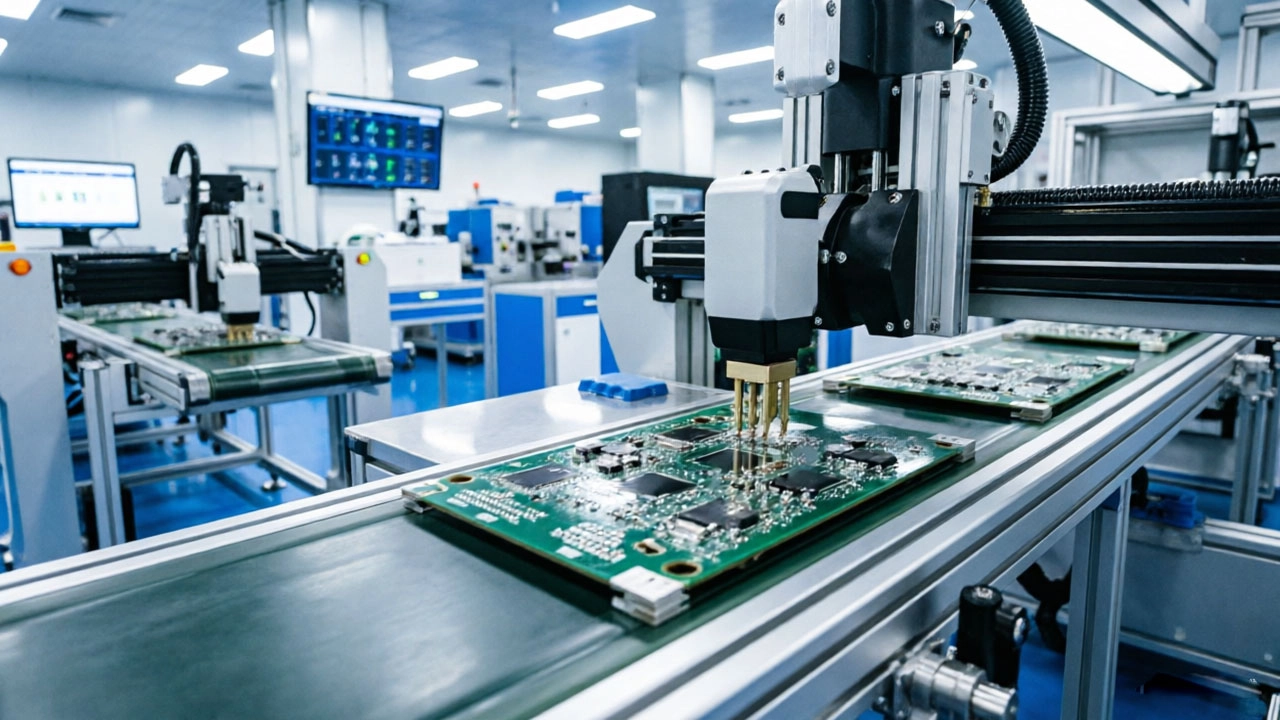
When you think of cutting-edge electronics, from AI servers to autonomous vehicles, one fundamental truth remains: they all rely on flawless circuit boards. But as components shrink to the size of a grain of sand, achieving perfect alignment is no longer just about having good machines. So, how do top-tier facilities maintain such exacting standards? The answer lies in understanding how Chinese manufacturers ensure precision in the SMT Pcb Assembly process today.
In this comprehensive guide, we will strip away the marketing fluff and dive into the actual engineering practices, real-world data, and shop-floor realities that drive high-yield manufacturing. Whether you are an OEM sourcing partners or an engineer optimizing your own lines, these insights will provide actionable value for your next project.
Precision starts long before the first chip is placed. Industry data consistently shows that over 70% of all soldering defects originate during the paste printing stage. Recognizing this, leading factories have moved beyond basic mechanical printers to fully automated systems with dynamic parameter compensation.
Practical Takeaway: Never assume your Pcb Design perfectly matches the manufacturer's capabilities. Always request a Design For Manufacturing (Dfm) review to verify pad sizes and clearances align with their specific stencil thickness and printer tolerances.
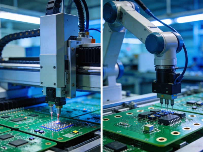
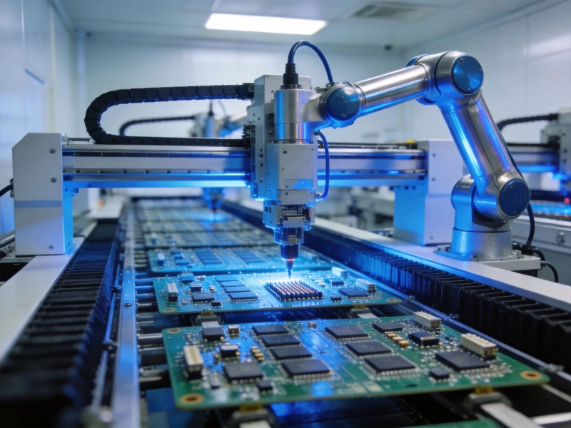
Placing 01005 components (measuring just 0.4mm x 0.2mm) requires equipment that operates in the sub-micron realm. Chinese PCBA leaders achieve this not just by buying expensive gear, but by mastering its application.
From my own experiance visiting production floors in Shenzhen, I've seen operators spend hours calibrating feeder slots. This meticulous attention to detail prevents micro-vibrations that could throw off placements at 80,000 CPH speeds.
Melting solder seems simple, but creating a reliable metallurgical bond without frying sensitive ICs is an art backed by thermodynamics. Top-tier Chinese manufacturers treat the reflow oven as a highly controlled chemical reactor rather than just a heater.
To guarantee uniformity, factories map thermal profiles using multi-channel dataloggers attached directly to dummy boards. Nitrogen environments are also standard practice, reducing oxygen levels to under 100 PPM to minimize oxidation and improve wetting angles.
Precision means nothing if hidden defects slip through. The quality assurance ecosystem in China has evolved far beyond human inspectors staring at magnifying glasses.
Achieving micron-level accuracy in Surface Mount Technology is a symphony of material science, mechanical engineering, and software intelligence. Chinese manufacturers have proven they can deliver world-class precision by combining state-of-the-art hardware with relentless process discipline and statistical control.
Ready to elevate your next hardware build? Don't settle for generic quotes. Reach out to our engineering team today to discuss your specific Dfm requirements and discover how our precision SMT capabilities can bring your designs to life flawlessly.
Q1: What is the smallest component size currently supported in mass production?
Yes, leading facilities routinely handle 01005 (0.4x0.2mm) and even 008004 components. However, achieving high yield at this scale requires specialized stencils and optimized reflow profiles.
Q2: How do factories prevent moisture-related defects like popcorn effect?
Strict humidity control (40-60% RH) and MSL (Moisture Sensitivity Level) tracking are enforced. Components exceeding their floor life are automatically routed to industrial ovens for baking before assembly.
Q3: Can I get full traceability for every single board produced?
Absolutely. Modern MES (Manufacturing Execution Systems) link every serial number to specific machine parameters, solder paste batch numbers, and AOI results, providing complete lifecycle transparency.

The Importance of BOM Accuracy in the PCB Assembly ProcessJuly/13/2026
Managing Cost and Quality in Quick Turn PCBsJune/04/2026
SMT vs THT PCB Assembly in China: Which Technology is Right for Your Project?June/10/2026
The Benefits of Combining PCB Fabrication and AssemblyMay/22/2026
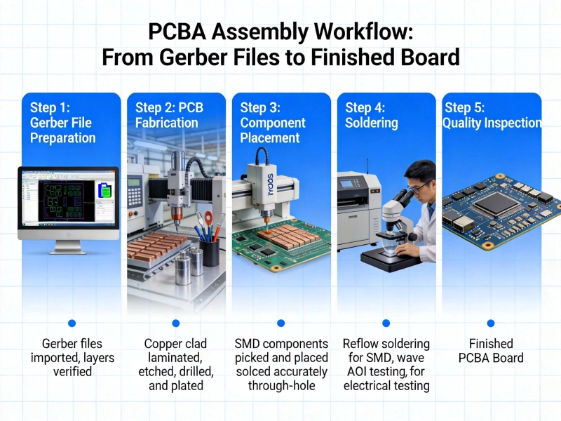
Understanding the PCBA Workflow: From Gerber Files to Finished BoardJune/16/2026
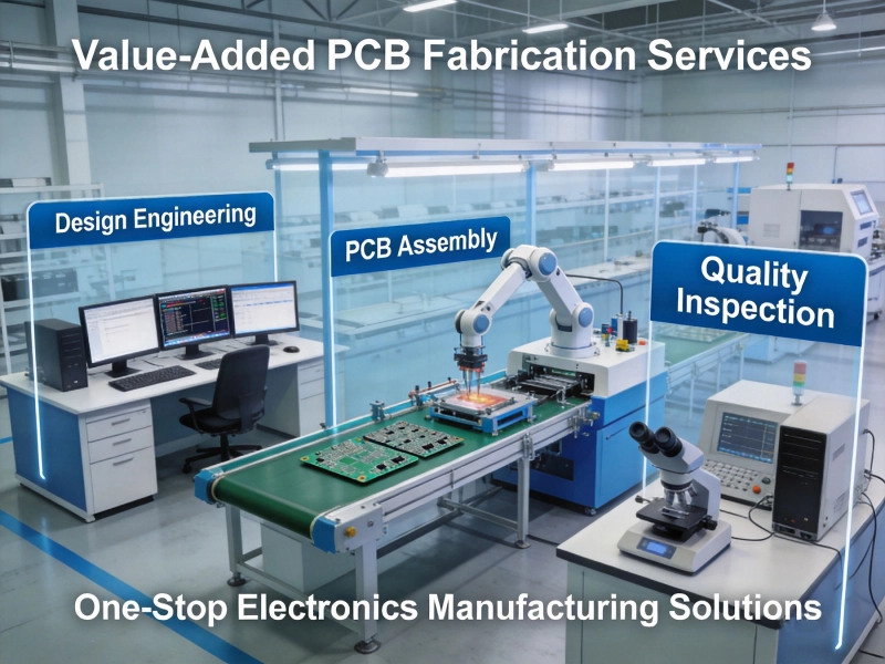
Value-Added PCB Fabrication Services: Beyond Just Making the BoardJune/12/2026
8-Layer vs. 16-Layer: Deciding on the Right Stack-up for Your Multilayer BoardJune/27/2026
Heavy Copper PCBs: Capabilities for High-Current and Power ElectronicsJuly/14/2026