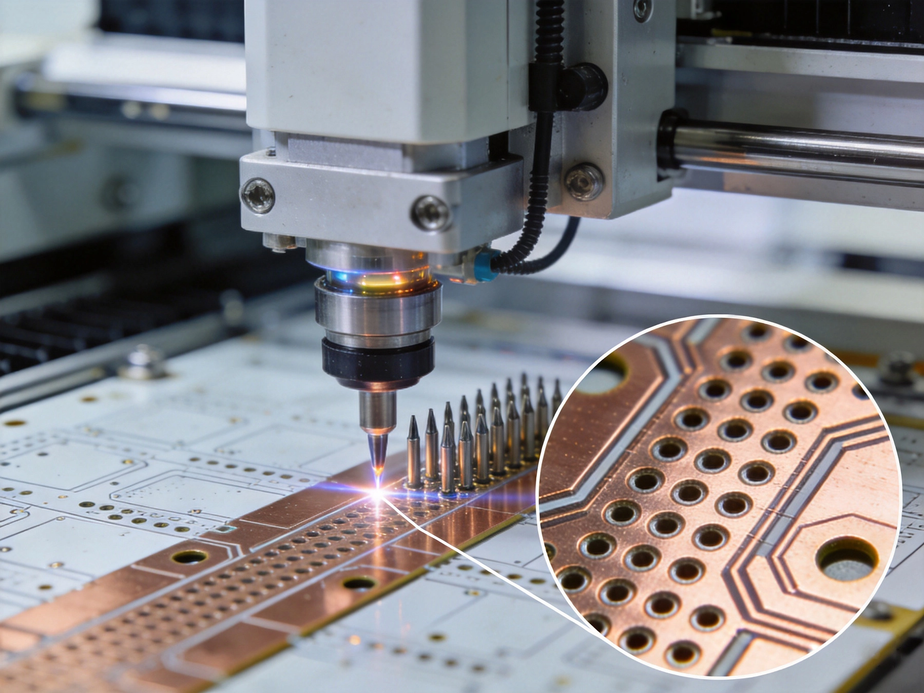
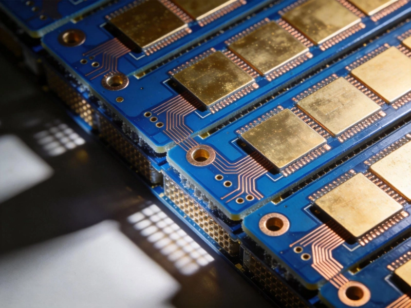
Drilling ranks among the most technically demanding operations in Pcb Manufacturing. Every plated through-hole, blind via, and buried via begins as a drilled entry point in the laminate substrate, and the precision of that drilling directly determines electrical reliability, manufacturing yield, and ultimately the cost structure of the finished board. As electronic devices have shrunk and their functionality expanded, the drilling process has evolved from simple mechanical puncturing into a sophisticated discipline combining precision engineering, materials science, and advanced process control.
The choice between mechanical drilling and laser drilling represents a fundamental decision point in Pcb Design and manufacturing. Each approach offers distinct advantages, carries specific limitations, and suits different application categories. Understanding the art and science behind both methods helps engineers and procurement professionals make informed decisions that balance performance requirements against cost and producibility constraints.
Before comparing drilling techniques, recognizing the via types that require drilling clarifies why the choice matters. Through-hole vias penetrate the entire board thickness, connecting outer layers to all inner layers. These holes serve both mechanical component mounting and electrical interconnection purposes, with diameters ranging from 0.25 mm for surface-mount assemblies to several millimeters for large connectors and power applications.
Blind vias connect an outer layer to one or more inner layers without reaching the opposite outer surface. These structures enable higher routing density by freeing up board real estate that through-holes would otherwise consume. Blind via formation requires either controlled depth drilling, sequential lamination, or laser ablation techniques depending on the specific manufacturing approach.
Buried vias reside entirely within inner layers, connecting internal planes and traces without reaching either outer surface. These structures enable complex multilayer designs with dense routing, but require formation during the inner-layer build-up process before outer layers are laminated. Laser drilling has become the dominant technology for buried via formation due to its ability to precisely ablate dielectric material without disturbing surrounding copper structures.
Microvias represent the smallest via category, typically defined as holes below 0.15 mm diameter serving connections between adjacent layers in HDI (High Density Interconnect) designs. The term microvia often implies laser-formed structures, though mechanical drilling can produce microvias with appropriate equipment. The distinction between microvia and standard via frequently relates more to aspect ratio and application context than absolute dimension.
Mechanical drilling uses rotating cutting tools to remove material from the PCB substrate, creating holes through the full board thickness or to controlled depths for blind via applications. The drilling system employs computer-controlled multi-spindle machines that position the board under precision guidance, advancing drill bits through the stack at controlled feed rates optimized for the specific material composition.
Drill bits for PCB applications utilize tungsten carbide or polycrystalline diamond (PCD) cutting edges mounted on steel bodies. Carbide bits offer excellent sharpness and wear resistance for standard materials including FR-4, Polyimide, and hydrocarbon laminates. PCD bits provide superior wear life for challenging materials such as ceramic-filled substrates, though at significantly higher cost that limits use to high-volume production runs.
The drilling process generates substantial heat at the cutting edge, requiring careful management to prevent resin softening, smearing across hole walls, and compromised plating adhesion. Dust collection systems continuously evacuate chips from the drilling zone, while peck drilling cycles periodically retract the bit to clear accumulated debris. Cooling strategies range from air blast to specialized drilling fluids that improve hole wall quality on critical applications.
Mechanical drilling handles a wide range of hole sizes, from sub-0.2 mm diameters for fine-pitch components to several centimeters for large mechanical mounting holes. Aspect ratios—the ratio of hole depth to diameter—can reach 20:1 or higher for standard through-holes, though drilling small high-aspect holes presents increasing challenges as depth increases. Hole location accuracy of ±0.05 mm is achievable with modern CNC equipment, meeting requirements for most consumer, industrial, and telecommunications applications.
Mechanical drilling introduces钻孔 taper—the hole diameter at the board top differs slightly from the bottom due to drill deflection and pressure variations. For standard through-holes, this taper presents no functional concern since plating conformality fills the minor diameter variations. However, high-frequency applications operating above 10 GHz can experience signal degradation from rough hole walls created by mechanical drilling, particularly when debris remains embedded in the dielectric material.
Stack drilling—simultaneously drilling multiple panels stacked together—improves throughput for identical designs but requires careful control of panel flatness and backup material quality. Stacked drilling introduces slightly larger hole size variation compared to single-panel drilling, limiting this technique to applications where extreme precision is not critical.
Laser drilling uses focused light energy to ablate—vaporize or sublime—dielectric material from specific locations, creating vias without physical cutting forces. Different laser types suit different material and via geometry requirements. CO2 lasers with 10.6 micrometer wavelength ablate organic dielectrics including FR-4, Polyimide, and hydrocarbon materials efficiently but poorly penetrate copper, requiring desmear processes to remove recast material from hole walls.
UV lasers operating at 355 nm wavelength cut through both dielectric and thin copper layers directly, enabling true copper-via formation without separate desmear processing. The shorter wavelength provides smaller heat-affected zones, producing cleaner hole walls with minimal recast material. UV laser systems are more expensive to acquire and operate but provide superior quality for microvia applications where hole wall quality directly impacts reliability.
YAG (yttrium aluminum garnet) lasers operating at 532 nm or 1064 nm wavelengths serve specialized applications, with green wavelength variants offering intermediate characteristics between CO2 and UV systems. The choice between laser types involves trade-offs between speed, hole wall quality, copper compatibility, and capital/operating costs.
Through-via laser drilling using CO2 systems typically employs a conformal mask or ablation technique where copper foil acts as the etch mask. The laser first perforates the copper layer in a defined pattern, then pulses continue to ablate dielectric material to the target depth. Multiple passes with decreasing energy density produce smoother walls than single-pass ablation, at the cost of additional process time.
UV lasers enable direct drilling through thin copper foils (typically 5-12 micrometers on HDI substrates) without separate copper patterning steps. This capability simplifies process flow and reduces registration challenges between drilling and copper etch operations. Direct laser drilling through copper works reliably for thin foils but becomes problematic for heavier copper weights where excessive pulses risk damaging surrounding circuitry.
Controlled depth drilling using laser energy requires real-time monitoring to detect when ablation reaches the target layer. Reflected light sensors detect the interface between dielectric and copper, triggering automatic process termination. This closed-loop control achieves depth accuracy of ±10 micrometers, far superior to mechanical blind via drilling that relies on stack height calibration and drill wear compensation.
Laser drilling produces significantly smaller holes than mechanical alternatives, with microvia diameters below 50 micrometers readily achievable. Hole wall quality excels due to minimal thermal damage zone, particularly with UV laser systems that vaporize material rather than melting it. Aspect ratios of 1:1 to 2:1 suit laser-formed microvias ideally, with no practical upper limit on achievable ratios since ablation depth controls precisely rather than drill penetration mechanics.
The non-contact nature of laser drilling eliminates mechanical stress on the PCB, preventing panel bowing and reducing handling-related defects. Multi-beam laser systems with parallel processing heads improve throughput for high-volume microvia production, though absolute speed remains slower than mechanical drilling for standard through-holes.
Laser drilling costs exceed mechanical drilling on a per-hole basis due to higher equipment investment, slower processing speed, and more expensive consumables (laser sources require periodic replacement). These cost differences diminish for high-density designs where laser drilling replaces multiple mechanical drilling and back-drilling operations, or where the electrical performance benefits justify premium pricing.
Mechanical drilling produces rough hole walls with vertical striations from cutter rotation, and drilling debris frequently accumulates in holes despite dust extraction systems. The desmear process—chemical or plasma treatment to remove smeared resin and debris—becomes essential preparation for plating adhesion on mechanically drilled holes. Without effective desmear, plating may separate from the hole wall during thermal cycling, creating reliability failures that manifest months after field deployment.
Laser drilling produces markedly smoother hole walls with minimal recast material when properly optimized. The precision of laser energy delivery eliminates smeared resin problems that plague mechanical drilling, though some CO2 laser applications still benefit from brief desmear processing to ensure maximum plating adhesion. The cleaner interface between dielectric and copper promotes more reliable plating coverage, particularly important for thermal cycling reliability in automotive and aerospace applications.
Mechanical drilling accuracy depends on machine calibration, drill wear, and panel handling consistency. Modern CNC drilling systems achieve registration accuracy of 0.05 mm or better for standard through-holes, sufficient for most applications. Blind via drilling accuracy degrades with depth into the panel due to drill deflection, requiring tighter tolerances than the nominal machine accuracy might suggest.
Laser drilling registration follows the inner-layer artwork directly, since the laser targets copper-defined locations without intermediate positioning steps that accumulate error. This inherent registration advantage proves critical for HDI designs with fine-pitch components where pad diameters leave minimal margin for misregistration. Laser-formed microvia placement typically achieves accuracy below 0.02 mm, enabling component pitches of 0.3 mm and finer that would challenge mechanical drilling capabilities.
Mechanically drilled and plated through-holes have demonstrated decades of field reliability when properly processed. The IPC Class 3 requirements for high-reliability applications specify plating thickness, desmear completeness, and testing protocols that ensure reliable performance under thermal cycling, vibration, and humidity exposure. Military and aerospace standards push requirements higher still, with extended thermal cycling and vibration testing validating designs before production release.
Laser-formed microvias have faced historical skepticism regarding long-term reliability, but extensive qualification data from HDI product deployments over the past fifteen years has largely dispelled reliability concerns when manufacturing processes meet established standards. Microvia reliability benefits from the absence of glass fiber interruption (common in mechanically drilled holes that intersect woven reinforcement patterns) and from superior plating adhesion to laser-cleaned surfaces.
Mechanical drilling equipment ranges from modest single-spindle machines suitable for Prototype and low-volume production to high-speed gang drills with twenty or more spindles for high-volume standard PCB production. A capable precision CNC drilling system suitable for commercial PCB production costs between $150,000 and $500,000, while high-throughput production machines can exceed $1 million. Operating costs center on drill bit consumption, with carbide bits lasting 500-2000 hits depending on material and hole size, while PCD bits last significantly longer at premium pricing.
Laser drilling systems command substantially higher investment, with CO2 laser drill systems starting above $500,000 and advanced UV laser systems frequently exceeding $1.5 million. Operating costs include laser source replacement (typically required every 2,000-5,000 hours), process gases for UV systems, and generally higher maintenance requirements than mechanical equipment. Despite these costs, laser drilling remains economically justified for HDI production where the alternative of sequential lamination and mechanical drilling incurs its own substantial costs.
Low-volume Prototype production favors mechanical drilling due to lower setup costs and faster job changeover times. Loading a new drill program and changing bits for different hole sizes takes minutes, while laser system job changes involving beam alignment verification and process optimization can extend setup times considerably. For prototype quantities under 25 pieces, mechanical drilling typically provides faster delivery schedules.
High-volume production of standard PCBs benefits from mechanical drilling throughput advantages, where gang drills can produce hundreds of holes per minute across stacked panels. Laser drilling throughput, while improved with multi-beam systems, generally cannot match mechanical drilling for high-hole-count standard designs. The crossover point where laser becomes cost-competitive depends on specific board complexity, hole count, and the density advantages laser drilling provides for HDI designs.
Modern HDI PCB production frequently employs both mechanical and laser drilling in the same board, using each technology where it provides the best economic or performance outcome. Standard through-holes, mounting holes, and larger interconnects typically route to mechanical drilling, while fine-pitch blind and buried microvias receive laser processing.
Sequential lamination builds complex HDI structures where inner-layer microvias form through laser ablation before outer layers are laminated, then outer-layer mechanical drilling creates larger through-connections that link the laser-formed internal networks. This hybrid approach leverages the precision of laser drilling for density-critical structures while accepting the cost-effectiveness of mechanical drilling for connections where precision requirements are less demanding.
The decision sequence for hybrid manufacturing planning typically begins with identifying microvia locations and dimensions, then determining whether laser drilling provides necessary precision or whether mechanical blind via drilling can meet requirements with lower cost. Through-hole requirements subsequently allocate to mechanical drilling, potentially with back-drilling for high-frequency applications requiring stub removal. This systematic approach optimizes the technology mix for each specific design.
Mechanical drilling remains the workhorse technology for through-hole formation, mounting holes, and applications where hole size and depth tolerances permit. The technology is well-understood, equipment is widely available, and per-hole costs scale favorably for high-volume production of standard designs. Appropriate desmear and plating processes ensure reliable electrical connections that meet decades of field-proven performance standards.
Laser drilling provides precision and capability that mechanical drilling cannot match for microvia formation, enabling HDI designs with densities impossible through conventional through-hole approaches alone. Superior hole wall quality, excellent registration accuracy, and the flexibility to form blind and buried vias in controlled depths justify premium costs for applications requiring these capabilities.
The art of PCB drilling lies in selecting the appropriate technology—or optimal combination of technologies—for each specific design requirement. Working with manufacturing partners who possess both capabilities enables design optimization that leverages each method's strengths without forcing compromises that sacrifice performance or inflate costs unnecessarily.
Mechanical drilling reliably produces holes down to approximately 0.15 mm diameter in production quantities, with some advanced equipment achieving 0.1 mm for specialized applications. Below this range, drill breakage rates become prohibitive for commercial production, making laser drilling the practical choice for microvia formation.
Microvia dimensions typically fall below 0.15 mm diameter with depth of 0.05-0.15 mm, creating aspect ratios and physical scales that exceed mechanical drilling capabilities. Laser drilling achieves these dimensions reliably, while the clean hole walls and excellent registration accuracy laser provides prove essential for the component densities HDI designs target.
Laser drilling cannot economically replace mechanical drilling for larger holes, mounting holes, and standard through-holes where mechanical drilling provides adequate quality at far lower cost. The two technologies complement each other, with laser serving precision microvia requirements and mechanical drilling handling larger features efficiently.
Mechanical drilling cost scales primarily with hole count and aspect ratio, with larger and deeper holes requiring more expensive bits and slower processing. Laser drilling cost scales with hole count, hole size, and depth, with smaller and shallower holes processing faster. The cost crossover depends on specific design parameters but generally favors mechanical drilling for holes above 0.25 mm diameter.
IPC standards specify thermal cycling tests, daisy chain pull testing for vias, cross-section analysis of hole wall quality, and plating thickness verification. High-reliability applications add extended thermal cycling, vibration testing, and humidity exposure protocols. X-ray inspection verifies internal hole quality and plating coverage, particularly important for blind and buried vias that cannot be inspected from the surface.

How AI-Driven Scheduling is Making Rapid PCB Prototyping More ReliableJune/18/2026
A Step-by-Step Walkthrough of the PCB Fabrication ProcessMay/21/2026
Understanding the PCBA Workflow: From Gerber Files to Finished BoardJune/16/2026
Decoding the Spec Sheet: Understanding a Factory's PCB Fabrication CapabilitiesJune/11/2026
The Advantages of HDI PCB Fabrication for Compact ElectronicsMay/22/2026
How Chinese Manufacturers Ensure Precision in the SMT PCB Assembly ProcessJune/03/2026
Copper Pour vs Trace for High Current: Optimizing PCB Power Delivery and Thermal ManagementJune/11/2026

The Rise of Smart Factories: How Automation is Revolutionizing China's PCB SectorJune/16/2026