High-speed digital designs operating at multi-gigabit data rates demand Signal Integrity performance that conventional PCB via structures simply cannot deliver. Signal frequencies in modern interfaces such as PCIe 5.0/6.0, 400G Ethernet, DDR5, and USB4 push well into the tens of GHz, where even minor impedance discontinuities caused by via stubs and via transitions can degrade signal quality beyond recovery. Back-drilling and via-in-pad are two advanced via technologies that address these challenges, enabling high-speed signals to transition between PCB layers with minimal reflection, attenuation, and crosstalk. Understanding when and how to apply these techniques is essential for any engineer working on High-speed Pcb designs.

The Signal Integrity Problem with Standard Vias
In a standard through-hole via, the drilled hole passes through all layers of the PCB, even when the signal only needs to transition between two specific layers. The portion of the via barrel that extends beyond the signal connection point—known as the via stub—acts as an unterminated transmission line stub that causes significant Signal Integrity problems at high frequencies.
How Via Stubs Degrade Signal Integrity
- Resonance Effects: The via stub behaves as a resonant structure with a quarter-wavelength resonance frequency determined by the stub length and the effective Dielectric Constant of the surrounding material. At the resonance frequency, the stub presents a low-impedance path to ground, causing severe signal attenuation—a phenomenon known as stub resonance. For a 10mil stub in a typical FR-4 stackup, the first resonance occurs around 40-50GHz, but longer stubs in thick boards can resonate at much lower frequencies that fall within the operating band of high-speed signals.
- Impedance Discontinuity: The via barrel, anti-pad, and pad stack create an impedance discontinuity in the signal path, causing partial signal reflection. The reflected energy reduces the signal amplitude arriving at the receiver and can cause inter-symbol interference (ISI) that degrades bit error rate performance.
- Increased Insertion Loss: Energy radiated from the stub and dissipated in the surrounding dielectric material increases insertion loss, reducing the signal amplitude that reaches the receiver. This loss increases with frequency, limiting the maximum usable bandwidth of the interconnect.
- Crosstalk Coupling: Stub portions of adjacent vias can couple electromagnetically, causing crosstalk between signals on different nets that would otherwise be well-isolated. This coupling increases with frequency and stub length.
For signals operating below 1-2GHz, via stub effects are generally negligible. But for multi-gigabit signals, stubs as short as 5-10mils can cause measurable degradation, and stubs of 50-100mils or more in thick Multilayer Boards can be catastrophic.
Back-Drilling: Eliminating Via Stubs with Controlled-Depth Drilling
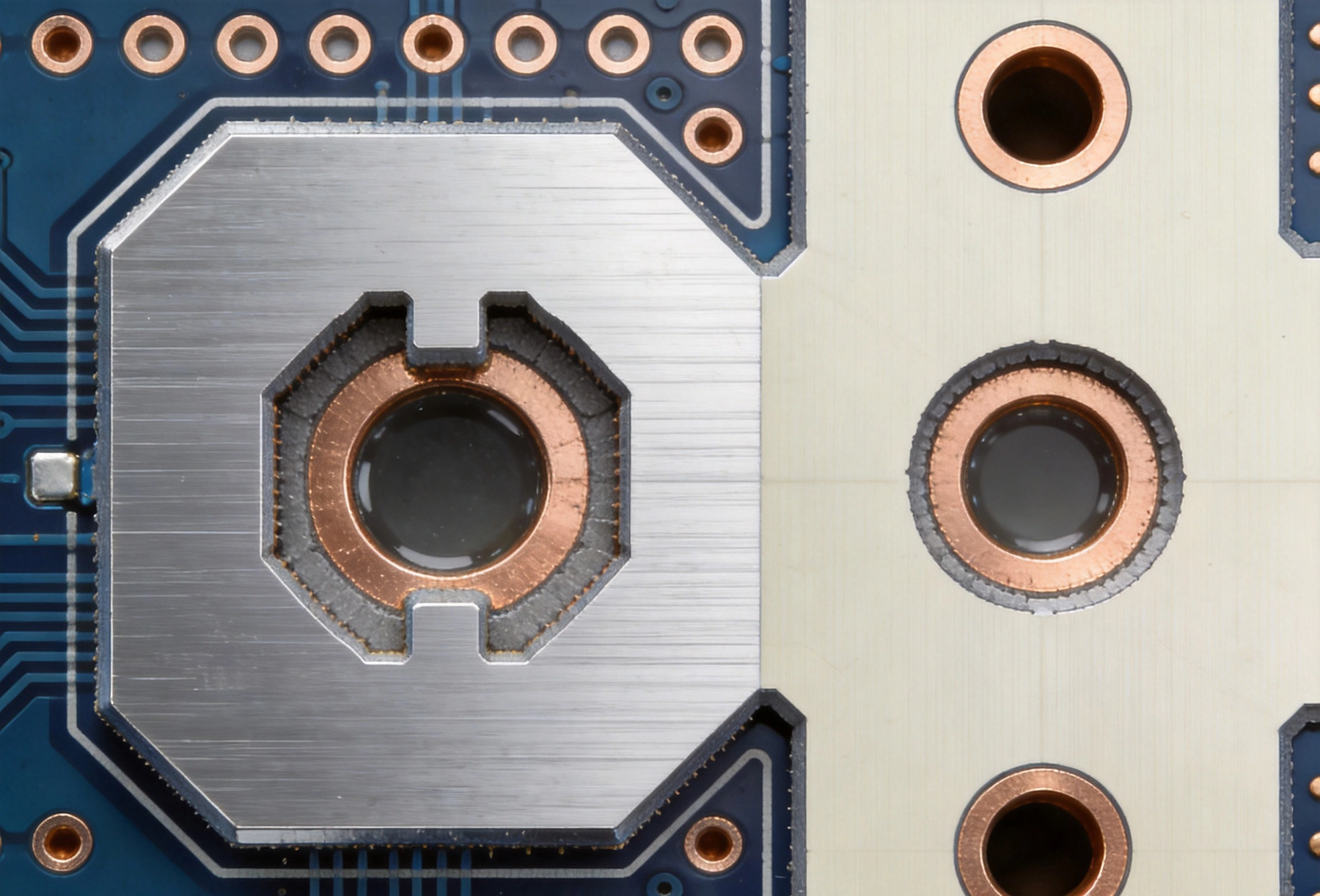
Back-drilling (also called controlled-depth drilling or stub removal) is a post-lamination manufacturing process that removes the unused portion of a through-hole via barrel by drilling from one side of the board to a controlled depth that just past the last signal layer connection.
How Back-Drilling Works
- After standard through-hole drilling and plating, a second drilling operation is performed from the back side of the board using a slightly larger drill bit (typically 2-4mil larger than the original via diameter)
- The back-drill depth is controlled to remove the copper barrel from the stub portion while preserving the electrical connection to the target signal layer
- The resulting via has a shortened barrel that extends only to the last required connection layer, with the stub portion completely removed
- Residual stub length after back-drilling is typically 5-10mil, limited by drill depth tolerance and the need to preserve the connection to the target layer
Benefits of Back-Drilling
- Elimination of Stub Resonance: By removing the majority of the via stub, back-drilling pushes the stub resonance frequency well above the operating frequency of the signal, eliminating resonance-related attenuation. A 5mil residual stub resonates around 80-100GHz, far above the operating range of even the fastest current interfaces.
- Improved Signal Integrity: Reduced impedance discontinuity and elimination of stub resonance result in cleaner signal transitions with less reflection, lower insertion loss, and wider open eye diagrams at the receiver.
- Reduced Crosstalk: Shorter via barrels reduce electromagnetic coupling between adjacent vias, improving crosstalk performance in dense high-speed routing areas.
- Compatibility with Existing Design Flows: Back-drilling does not require changes to via pad sizes or anti-pad dimensions, making it relatively easy to implement in existing designs as a manufacturing specification.
- Cost-Effective for Selected Vias: Back-drilling can be applied selectively to only the vias that carry high-speed signals, avoiding the cost penalty of applying it to all vias on the board.
Back-Drilling Design and Manufacturing Considerations
- Drill Depth Tolerance: The back-drill depth must be controlled within tight tolerances (typically ±3mil) to ensure the stub is removed without cutting into the target layer connection. Tighter tolerances increase manufacturing cost and may require specialized drilling equipment.
- Residual Stub Length: Even with perfect depth control, some residual stub remains due to the need to maintain adequate plating connection at the target layer. Design simulations should account for the residual stub length when predicting signal integrity performance.
- Increased Manufacturing Cost: Back-drilling adds a second drilling operation and requires additional setup and inspection, adding 5-15% to Pcb Manufacturing Cost depending on the number of vias to be back-drilled.
- Drill Bit Registration: The back-drill must be accurately aligned with the original via location. Misregistration can result in partial stub removal or damage to the target layer connection. Most fabricators maintain registration accuracy within 2-3mil.
- Multiple Back-Drill Depths: Designs with signals transitioning at different layers may require multiple back-drill depths on the same board, adding setup complexity and cost. Grouping signals to minimize the number of distinct back-drill depths reduces manufacturing complexity.
- Aspect Ratio Limitations: Back-drilling of very deep vias (high layer count boards) may be limited by drill bit aspect ratio constraints. Very long, thin drill bits can wander or break, limiting the maximum back-drill depth for small-diameter vias.
Via-in-Pad: Enabling High-Density BGA Breakout
Via-in-pad (also called via-in-pad-plated-over or VIPPO) places a via directly within a component landing pad, allowing the signal to transition to another layer immediately at the component connection point. This technique is essential for fine-pitch BGA breakout where routing space between adjacent pads is insufficient for a dog-bone fanout pattern.
The BGA Breakout Challenge
Modern BGA packages with pitches of 0.8mm, 0.65mm, and 0.5mm have extremely limited space between adjacent pads. In a traditional dog-bone fanout, a short trace routes from the BGA pad to a nearby via, but this requires space between pads that does not exist at fine pitches. Via-in-pad solves this by placing the via directly in the component pad, eliminating the need for fanout traces and enabling direct layer transition at the pad location.
Via-in-Pad Process Requirements
- Via Filling: The via hole must be filled with a non-conductive or conductive material to prevent solder from wicking into the via barrel during reflow, which would starve the solder joint of adequate volume and create an unreliable connection.
- Copper Capping: After filling, the via is plated over with copper to create a flat, solderable surface on the component pad. This copper cap must be sufficiently flat to ensure reliable solder joint formation with the BGA sphere.
- Surface Planarity: The filled and capped via-in-pad must meet surface planarity requirements (typically less than 25μm deviation) to ensure consistent solder paste deposition and reliable BGA solder joint formation across all pads.
Via Filling Methods
- Non-Conductive Epoxy Fill: The most common method, using epoxy resin to fill the via barrel before copper capping. Non-conductive fill is suitable for signal vias where the via does not need to carry high current between layers. The epoxy provides a solid, flat base for the copper cap but does not contribute to electrical conductivity or thermal transfer through the via.
- Conductive Copper Fill: Copper paste or electroplated copper fills the via barrel, providing both electrical continuity and thermal transfer through the via. Conductive fill is used for power and ground vias where the via must carry significant current between layers, or for thermal vias beneath power components that need to transfer heat to internal copper planes.
- Silver Epoxy Fill: A less common alternative using conductive silver epoxy that provides moderate electrical and thermal conductivity with easier processing than copper fill.
Benefits of Via-in-Pad
- Enables Fine-Pitch BGA Routing: Via-in-pad is often the only viable solution for routing signals from BGA packages with pitches below 0.8mm, where dog-bone fanout is impossible due to space constraints.
- Shorter Signal Paths: Direct layer transition at the component pad eliminates the fanout trace, reducing trace length and associated signal delay, attenuation, and crosstalk susceptibility. This is particularly beneficial for high-speed signals where every picosecond of skew and every dB of loss matters.
- Reduced Routing Congestion: Eliminating fanout traces significantly reduces routing congestion in the BGA breakout region, freeing routing resources for other signals and improving overall design routability.
- Improved Impedance Control: Shorter, more direct signal paths have fewer impedance discontinuities, improving signal integrity performance for high-speed interfaces.
- Thermal Transfer for Power Pads: Conductive-filled via-in-pad beneath component thermal pads provides a direct thermal path from the component to internal copper planes, significantly improving thermal performance compared to thermal vias placed beside the pad.
- Consistent Pad Geometry: All BGA pads have the same geometry with via-in-pad, simplifying design rule checking and ensuring consistent solder joint formation across all component connections.
Via-in-Pad Design and Manufacturing Considerations
- Increased Manufacturing Cost: Via filling and capping adds processing steps including via fill, planarization, and re-plating, adding 10-20% to Pcb Manufacturing Cost depending on the number of via-in-pads.
- Pad Flatness Requirements: The copper cap over a filled via must be flat enough to ensure reliable solder joint formation. IPC-4761 defines acceptance criteria for via-in-pad flatness that must be specified and verified.
- Via Size Constraints: The via diameter within a component pad is limited by the pad size. For very small pads (0.5mm pitch BGA), the via diameter may be only 0.2-0.25mm, approaching manufacturing capability limits for reliable filling and capping.
- Thermal Reliability: Differences in CTE between the fill material and the surrounding copper and laminate can cause reliability issues during thermal cycling. Conductive copper fill generally provides better CTE matching than non-conductive epoxy fill, but both are widely qualified for production use.
- Inspection Challenges: The quality of the via fill and copper cap cannot be easily inspected after manufacturing, making process qualification and statistical process control critical for reliable production.
- Rework Difficulty: BGA components mounted on via-in-pad locations are more difficult to rework because the via fill provides additional thermal mass that slows heating during rework reflow, potentially requiring adjusted rework profiles.
Combining Back-Drilling and Via-in-Pad
In advanced high-speed designs, back-drilling and via-in-pad are often used together to achieve optimal signal integrity:
- Via-in-Pad with Back-Drilling: For high-speed BGA signals, the via-in-pad provides direct pad-to-layer transition, while back-drilling removes the stub from the via-in-pad to eliminate stub resonance. This combination provides the shortest possible signal path with no stub-related degradation.
- Design Flow Integration: Modern EDA tools support combined specification of via-in-pad and back-drilling, allowing designers to define via structures that include both capabilities. The fabrication drawing must clearly specify which vias require via-in-pad construction and which require back-drilling, along with the back-drill depths for each group.
- Cost Optimization: Apply both techniques selectively—only to vias that carry high-speed signals or connect fine-pitch BGA pads. Using via-in-pad for all pads or back-drilling for all vias unnecessarily increases manufacturing cost.
Alternative Via Technologies
For designs where back-drilling and via-in-pad may not be the optimal solution, several alternative technologies address via-related signal integrity challenges:
- Blind and Buried Vias: Vias that span only specific layers of the stackup, completely avoiding stub formation by connecting only the layers they need. Blind/Buried Vias are the most effective solution for stub elimination but add significant manufacturing cost and design complexity, particularly for HDI constructions with multiple via levels.
- Microvias: Laser-drilled vias typically 0.1-0.15mm in diameter that span only one or two layers, used in HDI constructions. Microvias have no stub by definition and provide excellent signal integrity, but are limited in the number of layers they can span and require sequential lamination processing.
- Via Stagger and Shift: In multi-layer HDI constructions, staggering or shifting via positions between layers can reduce crosstalk coupling between adjacent via transitions while maintaining routing density.
Design Guidelines for High-Speed Via Structures
- Simulate Before You Build: Use 3D EM simulation to model via transitions including pads, anti-pads, barrels, and stubs to predict impedance, return loss, and insertion loss performance before committing to fabrication. Simulation is the only reliable way to optimize via geometry for specific high-speed interfaces.
- Minimize Via Pad Size: Smaller capture pads and antipads reduce the capacitive loading of the via, improving Impedance Matching. Work with your fabricator to determine the minimum reliable pad size for your via construction.
- Optimize Anti-Pad Clearance: The anti-pad (the void in the reference plane around the via) significantly affects via impedance. Larger anti-pads reduce capacitive loading but reduce ground plane copper. Simulation can identify the optimal anti-pad size for your target impedance.
- Use Reference Vias for Ground Return: Place ground return vias (grounded barrels connected to reference planes) adjacent to signal vias to provide low-inductance return current paths, reducing crosstalk and improving signal integrity.
- Group Signals by Transition Layer: Route high-speed signals to transition at the same layer to minimize the number of distinct back-drill depths required, simplifying manufacturing and reducing cost.
- Document Clearly: Clearly specify via construction requirements (via-in-pad fill type, back-drill depths, plating requirements) on fabrication drawings and in manufacturing notes. Ambiguous specifications lead to Manufacturing Errors and scrap.
Conclusion
Back-drilling and via-in-pad are indispensable techniques for High-speed Pcb designs operating at multi-gigabit data rates. Back-drilling eliminates the via stub resonance that degrades signal integrity at high frequencies, while via-in-pad enables fine-pitch BGA routing with minimal signal path length and impedance discontinuity. Both techniques add manufacturing cost but deliver signal integrity improvements that are often impossible to achieve through any other means. By understanding the principles, benefits, and limitations of each technique, and applying them selectively where they provide the greatest value, designers can achieve the signal integrity performance their high-speed interfaces demand while managing manufacturing cost and complexity.
Contact us to discuss your requirements.