The cost of an HDI or Multilayer Pcb is not a simple function of board size or layer count. It is the result of many interacting factors — some driven by your design choices, others by the capabilities and processes of the fabricator. Understanding these cost drivers is essential for engineers who need to balance performance requirements against budget constraints, especially in the transition from Prototype to production where cost optimization can make the difference between a viable product and one that never ships.
This article breaks down the major cost drivers in HDI and multilayer PCB Fabrication, explains why each factor affects price, and provides practical guidance on where you can save cost without sacrificing the electrical and thermal performance your design requires.

Layer Count: The Most Visible Cost Driver
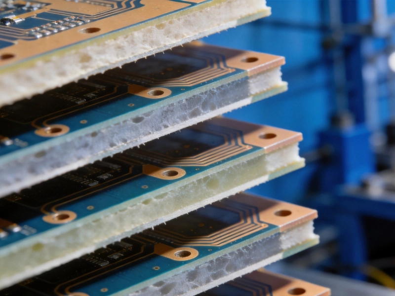
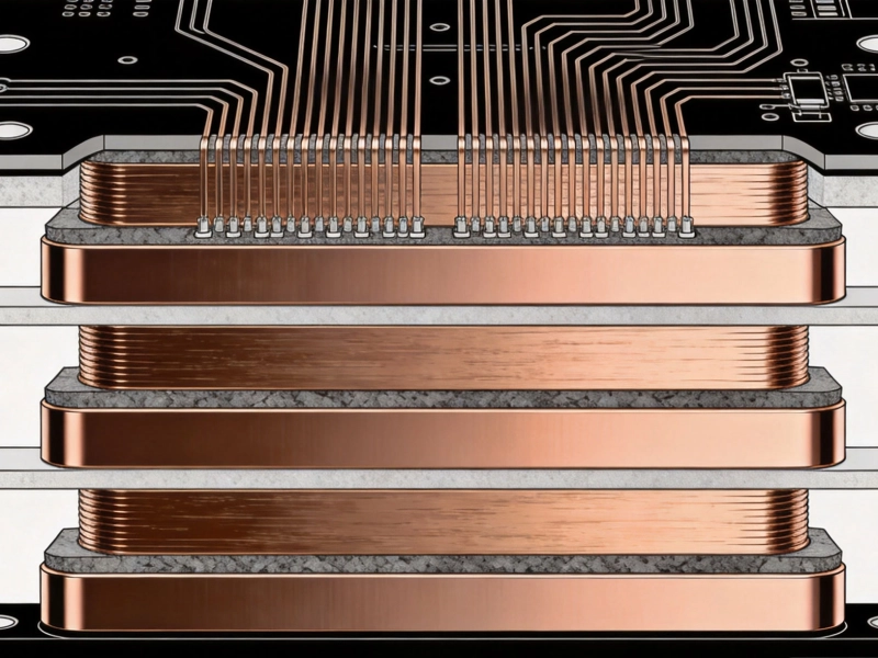
Every additional layer in a Multilayer Pcb adds material cost, processing steps, and yield risk. The relationship is not linear — it accelerates as layer count increases because higher layer count boards require more lamination cycles, more drilling, more plating, and more alignment steps, each of which can introduce defects.
How Layer Count Drives Cost
- Material cost: Each layer pair requires a core and Prepreg. A 4-layer board uses one core and two Prepreg sheets. An 8-layer board uses three cores and four prepreg sheets. Material cost scales roughly linearly with layer count, but specialty cores (high-Tg, low-Dk) add a premium per layer.
- Lamination cycles: Standard Multilayer Boards up to about 12 layers are typically laminated in a single press cycle. Beyond 12 layers, or when using HDI build-up constructions, multiple lamination cycles are required. Each additional lamination cycle adds processing time, energy cost, and yield risk.
- Registration difficulty: As layer count increases, maintaining alignment across all layers becomes more challenging. Misregistration between inner and outer layers can cause drill breakout on vias or misalignment of Controlled Impedance traces. Fabricators compensate with tighter process controls and larger annular rings, both of which add cost.
- Testing complexity: Each additional layer adds nets to be tested. Electrical test time and fixture complexity increase with layer count, especially for boards with dense BGA breakouts that require bed-of-nails or Flying Probe access.
Cost Optimization Tips for Layer Count
- Always question whether a layer can be eliminated. Can a signal be rerouted to share a layer? Can a split plane be merged? A 6-layer design that can be reduced to 4 layers typically saves 25-35 percent on fabrication cost.
- Use signal layer pairing effectively. In a 6-layer stack-up, two signal layers can share the space between two plane layers, giving good Impedance Control with fewer total layers than a design that dedicates a plane to every signal layer.
- For HDI designs, consider whether a Type I construction (one build-up layer on each side of a core) can replace a higher-order HDI type. Type I HDI with sequential lamination is significantly less expensive than Type II or Type III constructions that require multiple build-up cycles.
Via Technology: The Hidden Cost Multiplier
Via type and density are among the most underestimated cost drivers in HDI fabrication. The choice between through-hole vias, Blind Vias, Buried Vias, and Microvias — and the density at which they are used — can double or triple the cost of a board compared to a through-hole-only design.
Through-Hole Vias
Standard Plated Through-hole vias are the least expensive via type. They are drilled in a single operation, plated once, and require no sequential processing. The cost is driven primarily by the drill count and the aspect ratio (board thickness to drill diameter). High aspect ratio vias (above 8:1) require special plating processes to ensure reliable copper deposition in the via barrel, which adds cost.
Blind and Buried Vias
Blind Vias (visible from one side only) and Buried Vias (not visible from either side) require sequential lamination and drilling operations. Each additional drill pass adds setup time, processing time, and yield risk. The cost impact depends on the construction:
- Blind vias from outer to inner layers: Require controlled-depth drilling or Laser Drilling after the outer layers are laminated. Each blind via layer adds one drill pass and one plating operation.
- Buried vias between inner layers: Must be drilled and plated before the outer layers are laminated over them. This means the inner layer sub-assembly goes through a complete drill-plate-etch cycle before the final lamination. The extra processing steps add significant cost.
- Multiple via levels: A board with blind vias from L1-L2, L1-L3, and buried vias from L2-L5 requires three separate drill operations (plus the through-hole drill), each with its own setup, alignment, and plating step. This multiplies processing cost.
Microvias
Microvias (diameter ≤ 0.15 mm, typically laser-drilled) are the defining feature of HDI boards. Their cost impact comes from several factors:
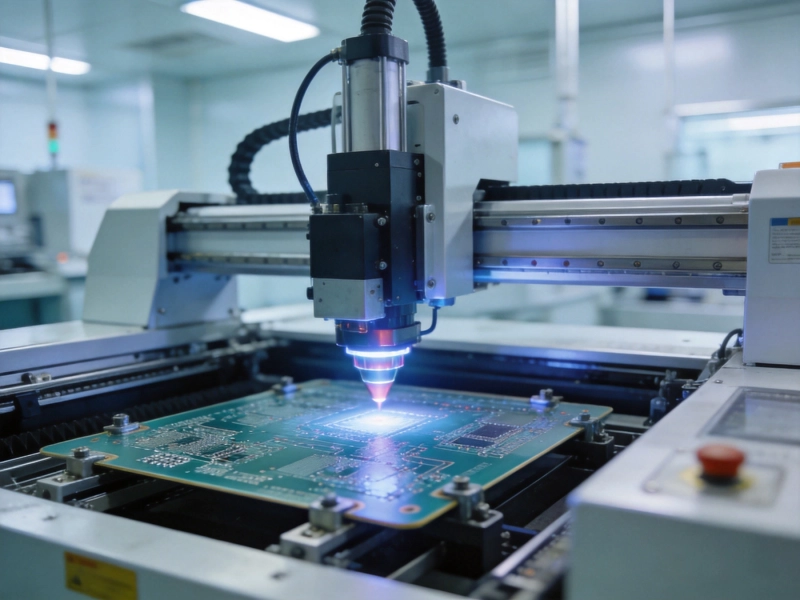
- Laser Drilling equipment: UV and CO2 laser drillers are expensive capital equipment. Fabricators charge a premium for laser drilling to recover this investment, and the per-via cost is higher than mechanical drilling.
- Via fill and capping: Microvias in via-in-pad constructions must be filled with copper or epoxy and planarized (capped) before the next layer is built up. This via fill process is an additional operation with its own materials, equipment, and yield challenges.
- Density and count: High microvia density increases per-board processing time on the laser driller. For designs with thousands of microvias, the laser drilling time alone can be a significant fraction of total processing time.
Cost Optimization Tips for Via Technology
- Minimize the number of different via types in a single design. A board that uses only through-hole and one level of blind vias is less expensive than one that uses through-hole, blind, buried, and microvias, even if the total via count is the same.
- Prefer via-in-pad with microvias only where necessary for BGA breakout. Not every fine-pitch BGA needs via-in-pad — many 0.5 mm pitch devices can be routed with dog-bone fanout using standard vias between pads.
- If your design uses stacked microvias (one via stacked directly on another), consider whether staggered microvias (offset vias connected by a short trace) would work instead. Staggered vias are easier to manufacture and have higher yield, which translates to lower cost.
Line Width and Spacing: The Precision Premium
Trace width and spacing directly affect the fabrication process capability required, and tighter geometries command a price premium. Standard fabrication capability at most shops is 4/4 mil (0.1/0.1 mm) trace/space. Going below this threshold — to 3/3 mil, 2/2 mil, or lower — pushes the fabricator into advanced capability territory, where yields drop and costs rise.
Why Tight Traces Cost More
- Etch factor compensation: As traces get narrower, the etch factor (lateral etching that makes trace width narrower than the Photolithography image) becomes a larger percentage of the trace width. Fabricators must compensate with over-sizing in the artwork, which requires tighter process control and more frequent measurement.
- Photolithography limits: Resolving fine features requires higher-resolution dry film or direct imaging (LDI) equipment. LDI is more expensive to operate than conventional contact printing with film artwork.
- Plating uniformity: For Controlled Impedance traces, plating thickness uniformity across the panel becomes more critical at finer line widths. Non-uniform plating that is acceptable at 5 mil traces may cause impedance violations at 3 mil traces.
- Yield loss: The defect rate for fine features is inherently higher. A single speck of dust on the photomask that would be inconsequential at 6 mil spacing can cause a short at 3 mil spacing. Lower yield means higher per-good-board cost.
Cost Optimization Tips for Trace Geometry
- Use the coarsest trace/space that meets your electrical requirements. For power traces, use wide traces. For controlled impedance signals, use the width that gives the target impedance with standard stack-up thicknesses — do not over-specify precision.
- If only a few traces require fine geometry (such as BGA breakouts), consider using a neck-down approach: route most of the trace at a wider width and narrow only in the breakout region. This reduces the area of the board that requires advanced processing.
- Check whether your fabricator's standard capability can handle your requirements before specifying advanced capability. Many designs specified at 3/3 mil can be reliably produced at 4/4 mil with slightly adjusted routing density.
Material Selection: Where Choices Compound
The laminate material system — core, prepreg, and copper foil — is a major cost driver, and the premium for specialty materials can be substantial. Standard FR4 (Tg ≈ 130-140°C) is the baseline. Moving to high-Tg FR4 (Tg ≈ 170°C), low-Dk/Df materials for high-frequency applications, or specialized laminates for HDI build-up each adds cost.
Material Cost Hierarchy
- Standard FR4 (Tg 130-140°C): Baseline cost. Widely available, mature Supply Chain, lowest price.
- High-Tg FR4 (Tg 170°C+): 20-40 percent premium over standard FR4. Required for lead-free assembly (higher reflow temperatures) and for boards that experience high operating temperatures or multiple reflow cycles.
- Mid-loss materials (Df ≈ 0.010-0.015): 50-100 percent premium over FR4. Used for high-speed digital applications (DDR4/5, PCIe Gen3/4) where Signal Integrity requires lower dielectric loss than standard FR4.
- Low-loss materials (Df ≈ 0.003-0.008): 100-300 percent premium. Required for RF/microwave and very high-speed applications (5G, mmWave, PCIe Gen5+).
- Specialty build-up dielectrics (ABF, RCC): 50-150 percent premium over standard prepreg. Used in HDI sequential lamination where the build-up layer requires a dielectric that can be laser-drilled reliably.
Copper Foil Type
Copper foil type also affects cost, especially for high-frequency and high-reliability applications:
- Standard electrodeposited (ED) copper: Lowest cost, standard for most applications. Higher roughness profile, which increases conductor loss at high frequencies.
- Low-profile copper (LP/VLP copper): 10-30 percent premium over standard ED foil. Smoother surface reduces conductor loss, important for signals above 5 GHz.
- Reverse-treated copper (RTF): Moderate premium. The rough side faces the laminate (for adhesion) while the smooth side faces the signal layer. A good balance of adhesion and low loss.
Cost Optimization Tips for Materials
- Do not over-specify material performance. If your design operates at frequencies where standard FR4 loss is acceptable, use FR4. Reserve low-loss materials for the layers that actually carry high-frequency signals.
- Consider hybrid stack-ups: use low-loss material only on the signal layers that need it, with standard FR4 on power and ground layers. This can cut material cost by 30-50 percent compared to an all-low-loss stack-up.
- For HDI build-up layers, confirm whether standard prepreg can be used instead of RCC (Resin-Coated Copper) or ABF. If laser drill capability is available for the chosen prepreg, avoiding specialty build-up materials saves significant cost.
Board Size, Panelization, and Utilization
The physical size of the board and how efficiently it fits on a fabrication panel directly affects per-unit cost. Fabricators process panels (typically 18×24 inches or 21×24 inches), and the number of boards per panel determines how the fixed processing cost is distributed.
Panel Utilization
A board that fits 10-up on a panel has its processing cost spread across 10 units. A board of slightly different dimensions that only fits 8-up pays the same panel processing cost over 8 units — a 25 percent higher per-board fabrication cost for the same work. This is one of the most impactful and least understood cost factors in PCB procurement.
Size-Related Cost Factors
- Large boards with low panel count: Boards approaching panel size (greater than 12×16 inches) may fit only 1- or 2-up, resulting in high per-unit processing cost.
- Odd-shaped outlines: Irregular board shapes that leave unused space on the panel reduce utilization. Adding breakaway tabs or designing with panelization-friendly outlines can improve utilization.
- Edge clearance requirements: Tooling holes, fiducials, and edge clearance for plating and Solder Mask reduce the usable panel area. These are necessary but reduce the number of boards per panel.
Cost Optimization Tips for Board Size
- Before finalizing board outline dimensions, ask your fabricator for panelization recommendations. A small adjustment in board width or height — even 5 mm — can sometimes increase the panel count significantly.
- Consider panelizing multiple different board designs on the same panel (mixed panelization) if you have several small boards for the same project. This can be especially cost-effective for low volume production.
- For very small boards, panelization with rout tabs or score lines is more cost-effective than individual board processing. Design your outlines to work with standard scoring or tab-routing patterns.
Surface Finish: Not All Finishes Cost the Same
The surface finish on external copper affects Solderability, shelf life, and cost. Your finish choice has both a direct cost impact and indirect implications for assembly yield.
- Hasl (Hot Air Solder Leveling): Lowest cost, but uneven surface and not suitable for fine-pitch components. Being phased out for lead-free assembly but still available in leaded Hasl for legacy designs.
- Lead-free HASL: Similar cost to leaded HASL. Wider variation in surface flatness compared to Enig, which can be problematic for components below 0.5 mm pitch.
- Enig (Electroless Nickel / Immersion Gold): 30-50 percent premium over HASL. Flat surface, excellent Solderability, long shelf life. The industry standard for most new designs. Risk of black pad defect if the nickel plating process is not well controlled.
- ENEPIG (Electroless Nickel / Electroless Palladium / Immersion Gold): 50-80 percent premium over HASL. Adds palladium layer between nickel and gold to prevent black pad. Used for high-reliability and wire-bonding applications.
- Osp (Organic Solderability Preservative): Similar cost to HASL, sometimes lower. Flat surface but limited shelf life (6-12 months) and not suitable for multiple reflow cycles. Good choice for single-sided assembly with Quick Turn time.
- Immersion Silver: Moderate cost, between HASL and ENIG. Good solderability and shelf life, but sensitive to handling and storage conditions. Can cause silver migration in high-humidity environments.
Yield and Its Impact on Effective Cost
Yield — the percentage of manufactured boards that pass all quality checks — is perhaps the most important and least visible cost driver. A board that costs $50 in materials and processing but has a 70 percent yield effectively costs $71.43 per good board ($50 / 0.70). The same board at 95 percent yield costs $52.63 per good board. Yield loss is an invisible cost that does not show up on the quote but shows up in the price you actually pay per usable unit.
Design Decisions That Affect Yield
- High aspect ratio vias (above 8:1): Plating voids and incomplete fill are more likely, reducing yield. Design with lower aspect ratios when board thickness allows.
- Fine line/space below fabricator standard capability: Every push beyond the manufacturer's sweet spot reduces yield. If you need 3/3 mil traces, make sure the fabricator has demonstrated high yield at that geometry — not just the capability to produce it.
- Stacked microvias: Stacked Vias are more susceptible to delamination and misalignment than staggered vias. The yield difference can be 5-15 percent, which significantly affects effective cost.
- Very large board size with many layers: Defect probability increases with board area and layer count. A defect that might be acceptable on a small board (if it falls in a non-critical area) may be a board-killer on a large, dense design.
- Tight impedance tolerance (±5 percent vs. ±10 percent): Tighter tolerances mean more boards fail impedance testing. If ±10 percent is acceptable for your design, do not specify ±5 percent.
Additional Process and Specification Cost Drivers
Beyond the major factors above, several additional specifications can add cost:
- Controlled impedance: Requires specific stack-up engineering, test coupons, and impedance testing. Adds 5-15 percent to board cost depending on the number of impedance targets and the tolerance required.
- Solder Mask color other than green: Red, blue, black, yellow, and white solder masks are available but may carry a small premium (5-10 percent) due to lower production volume at some fabricators.
- Multiple solder mask openings or defined pads: Solder mask defined pads (SMD) versus non-solder mask defined pads (NSMD) have different reliability implications but similar cost. Special openings for wave soldering or selective soldering add tooling complexity.
- UL recognition: Boards that require UL marking and recognition involve additional testing and documentation, adding cost and lead time.
- Electrical test complexity: Bare board Electrical Testing is standard, but the test method affects cost. Flying Probe testing is flexible but slower (higher per-board cost for large volumes). Fixture-based testing is faster for production but requires a one-time fixture cost.
FAQ
Does HDI always cost more than standard multilayer?
Not always. For a given routing density, an HDI board with fewer total layers may cost less than a standard Multilayer Board with many more layers. For example, a 6-layer HDI board with microvias might replace a 10-layer standard build. The HDI board has higher per-layer cost but fewer layers, and the total can be lower. The crossover point depends on the specific design, but it often falls in the 8-10 layer range for boards with high BGA density.
How much does panel utilization actually affect cost?
The impact can be dramatic. Going from 2-up to 3-up on a panel reduces per-board processing cost by roughly 33 percent, because the same panel processing (lamination, drilling, plating, etc.) is distributed over more units. For high volume production, even going from 8-up to 9-up saves about 11 percent. Always ask your fabricator for the optimal panelization for your board dimensions.
Is it worth paying for higher yield with a more capable fabricator?
For production volumes, absolutely. A fabricator that charges 20 percent more per board but achieves 95 percent yield versus 75 percent at a cheaper shop gives you a lower effective per-good-board cost ($1.20 × 1/0.95 = $1.26 vs $1.00 × 1/0.75 = $1.33). The higher-priced shop is actually cheaper per usable board. For prototypes, where you are buying a small fixed quantity, yield matters less because you are not paying per good board — you are paying per order. But for production, yield is king.
Can I reduce cost by specifying fewer electrical tests?
You can, but the risk is significant. Skipping Electrical Testing saves a small amount on fabrication but shifts the burden of defect detection to assembly, where the cost of finding and reworking a bare board defect is much higher. A single short between two nets that is not caught at bare board test can cause component damage during power-up that costs orders of magnitude more than the test you skipped. Electrical testing is one of the last places you should cut cost.
What is the single most impactful thing I can do to reduce PCB cost?
Reduce layer count. Every layer adds material, processing, testing, and yield risk. If you can eliminate even one layer through more efficient routing, plane merging, or use of HDI technology, the cost savings typically outweigh all other optimizations combined. Start your cost reduction effort by challenging every layer in the stack-up.
PCB Fabrication cost is driven by a complex interaction of design choices and manufacturing processes. Layer count, via technology, trace geometry, material selection, board size, surface finish, and yield all contribute to the final price — and many of these factors compound each other. A fine-line HDI board on low-loss material with stacked microvias hits every cost accelerator at once. The key to cost-effective design is understanding which factors matter most for your specific application and making informed trade-offs. Reduce layer count where possible, use the coarsest geometry that meets your requirements, select materials appropriate to your actual frequency needs, optimize panel utilization, and choose via technology that matches — rather than exceeds — your routing density needs. By treating cost as a design parameter rather than an afterthought, you can produce boards that meet all electrical and thermal requirements at a price that keeps your product competitive.
Contact us to discuss your requirements