Open Nav

No manufacturing process is perfect, and Pcb Assembly is no exception. Even in state-of-the-art facilities with automated lines and AI-powered inspection, defects occur — though at far lower rates than in facilities relying on older equipment or manual processes. The key difference between a high-quality manufacturer and a marginal one is not whether defects happen, but how systematically they prevent them, detect them, and eliminate their root causes.
For engineers, procurement managers, and product teams sourcing PCBA from contract manufacturers — especially in China — understanding the most common defect categories, why they occur, and how reputable factories prevent them is essential knowledge. This article provides a practical breakdown of the defect classes that matter most, with actionable insight into the prevention methods that separate reliable manufacturers from the rest.
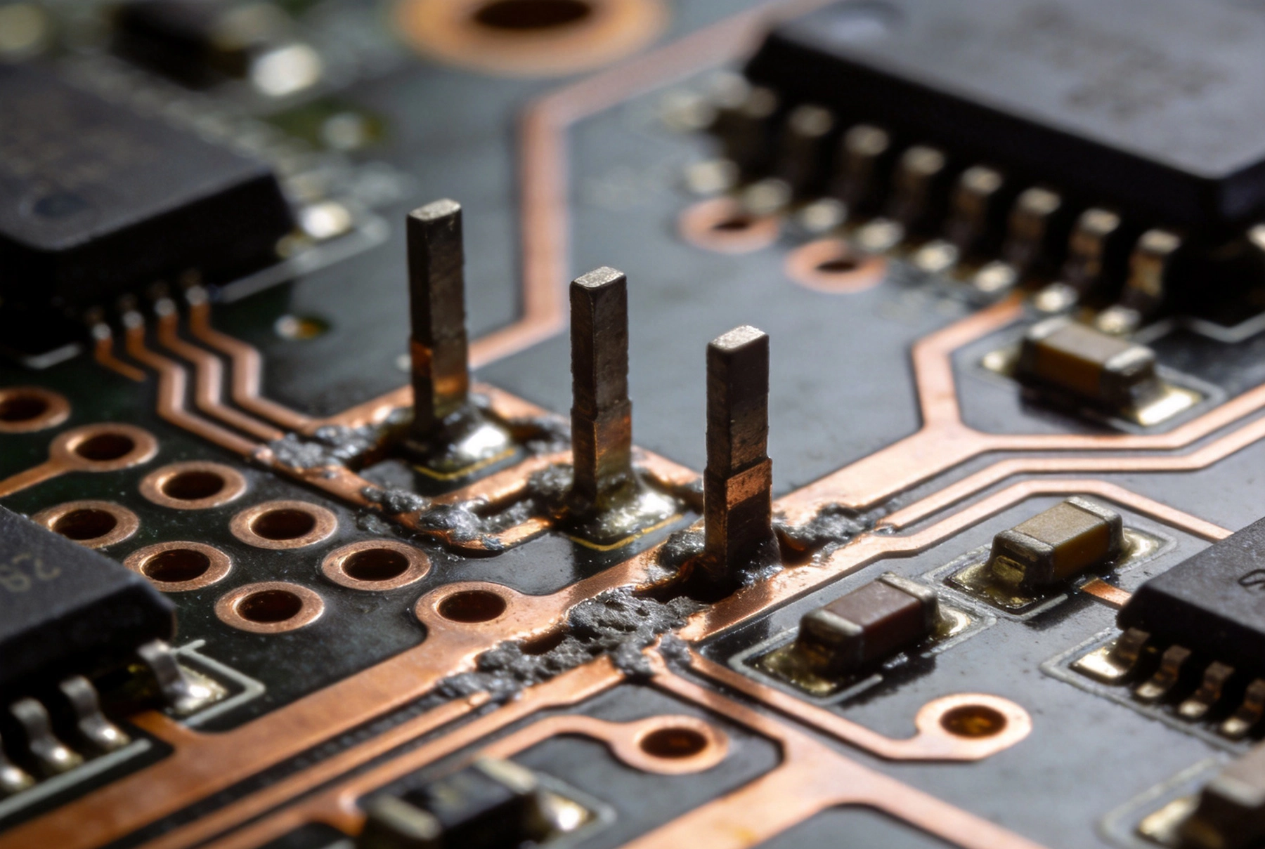
PCBA defects fall into several broad categories, each with different root causes, detection methods, and consequences. Some defects are purely cosmetic and have no functional impact. Others can cause intermittent failures that are extremely difficult to diagnose in the field. A few — particularly those affecting safety-critical systems — can have serious consequences.
The cost of a defect is not linear. A solder bridge that causes a board to fail final test costs the factory a few minutes of rework time. The same defect that escapes to the field in an automotive ECU can trigger a recall costing millions of dollars and irreparable damage to brand reputation. Understanding where on the cost curve a particular defect falls shapes how aggressively it should be prevented.
Solder is the fundamental joining material in Pcb Assembly, and defects related to solder — its application, formation, and integrity — account for the majority of assembly quality issues in most facilities.
A solder bridge occurs when solder connects two adjacent pads or leads that should remain electrically isolated. This is one of the most common defects in Surface Mount assembly, particularly for fine-pitch components like QFPs (Quad Flat Packages) and connectors with 0.5mm or 0.4mm lead spacing.
Root causes: Excess solder paste volume, stencil aperture misalignment, insufficient Solder Mask web between pads, or paste that is too fluid (due to incorrect viscosity or age). On the reflow side, a peak temperature that is too high or a time-above-liquidus that is too long can cause solder to flow beyond the intended pad area.
Prevention methods: Stencil aperture design is the first line of defense — apertures should be sized to apply exactly the right paste volume, with reductions for fine-pitch areas. Laser-cut stainless steel stencils with electropolished walls ensure clean paste release. Solder paste inspection (SPI) after printing, before reflow, catches 60–80% of potential bridge conditions before they become defects. A properly calibrated reflow profile with controlled peak temperature and time-above-liquidus prevents excessive solder flow during reflow.
A cold solder joint forms when solder does not melt fully or does not wet the pad and lead surfaces properly. The joint appears dull, grainy, or irregular rather than smooth and shiny. Cold joints have high electrical resistance and low mechanical strength, making them prone to failure under vibration, thermal cycling, or mechanical stress.
Root causes: Insufficient peak temperature during reflow, too-short time-above-liquidus, oxidized or contaminated pad or component lead surfaces, or solder paste that has been stored or handled incorrectly (improper refrigeration, exceeded shelf life, excessive exposure to humidity).
Prevention methods: Accurate profiling of the reflow oven using thermocouples on representative boards ensures the correct thermal profile is actually being achieved in production. Nitrogen inert atmosphere in the reflow zone reduces oxidation of solder and pad surfaces during reflow, particularly beneficial for gold-plated boards and Osp (Organic Solderability Preservative) finishes. Component and PCB storage per IPC/JEDEC standards — moisture-sensitive devices stored in dry cabinets, MSL-rated components baked before use — prevents moisture-related defects that can cause Solderability problems.
Tombstoning (also called drawbridging) occurs when one end of a two-terminal Surface Mount component — typically a resistor or capacitor — lifts off the pad during reflow while the other end remains soldered. The component stands up on one end like a tombstone. This defect is increasingly common as packages shrink and board density increases.
Root causes: Uneven heating of the component's two termination pads, causing one side to reflow before the other. Contributing factors include pad size mismatch between the two ends, unequal solder paste volume, uneven airflow in the reflow oven, and components placed off-center on the pads. Larger components with higher thermal mass are more susceptible because their ends heat at different rates.
Prevention methods: Matching pad designs on both ends of the component — same size, same thermal mass, same distance from thermal vias. Automated paste volume measurement on both pads to detect asymmetry before reflow. A well-designed reflow profile with a controlled preheat ramp prevents thermal gradients across the component. Component placement accuracy of ±0.05mm or better from modern pick-and-place machines eliminates placement offset as a contributing factor.
For components with exposed thermal pads — QFN, D2PAK, LGA packages — the solder joint under the thermal pad is critical for both electrical and thermal performance. Voiding occurs when air or Flux Residues become trapped in the solder joint during reflow, creating voids that reduce both mechanical strength and thermal conductivity.
Root causes: Insufficient solder paste coverage, inadequate flux outgassing pathways, or reflow profiles that ramp too quickly for trapped air and flux to escape before the solder solidifies.
Prevention methods: Thermal via arrays in the exposed pad footprint provide escape channels for outgassing. Optimized stencil aperture designs that achieve 75–85% coverage (rather than maximum coverage) allow flux to escape more readily. Vacuum-assisted reflow processes or void-reducing solder paste formulations can reduce voiding below 10%. X-ray Inspection of production samples verifies voiding rates against IPC-7095 standards.
Component placement accuracy is a function of the pick-and-place machine's precision, the accuracy of the component data (pickup location, fiducial recognition), and the condition of the feeder system. Even small offsets — 0.1mm to 0.2mm — can cause problems for fine-pitch components where the pad pitch is 0.4mm or less.
Root causes: Worn or misaligned feeders causing component pickup errors, fiducial mark recognition failures due to dirty or damaged fiducials, incorrect component data in the placement program, or warped boards that cause z-axis errors during placement.
Prevention methods: Vision systems on modern pick-and-place machines correct for component offset in real time by comparing the placed component's position against the pad. Global fiducial marks on the PCB provide a reference coordinate system that compensates for panel bow, warp, and cumulative placement errors. Regular feeder maintenance schedules and fiducial verification checks on every production run are standard practice in quality-focused factories. Board flatness verification before assembly — or specification of maximum bow-and-twist in fabrication — prevents z-axis errors that cause off-contact placement.
A component that fails to place — or places but does not bond due to no paste — is one of the simplest defects to detect and one of the most disruptive when it escapes to the field. Missing components are almost always caught at Aoi, but the question is whether the Aoi is placed at the right position in the process.
Root causes: Feeder failures (empty reel, tangled tape, malpositioned part), pick-up nozzle clogging, vacuum system failure, or a component that drops off during reflow due to insufficient paste.
Prevention methods: Feeder empty sensors on modern pick-and-place lines detect when a reel is running low or a tape has broken, pausing the line before a run of missing components is placed. AOI placed immediately after the pick-and-place step — before reflow — catches missing components before the board enters the oven, reducing scrap and rework cost. Statistical process control on component placement rates tracks feeder-related issues and triggers preventive maintenance before they cause defects.
Many defects go undetected not because they cannot be found, but because the inspection process does not cover them. AOI systems inspect for missing components, misalignments, and some solder defects, but they cannot see inside BGA packages, beneath QFN thermal pads, or through Multilayer Boards. X-ray Inspection, Ict (in-circuit test), and functional test are required to find the defects that AOI cannot see.
Root causes: Facilities that invest only in AOI and skip X-ray and Ict are essentially flying blind for certain defect categories. BGAs with hidden solder joint failures, buried shorts, and via barrel cracks are undetectable with optical inspection alone.
Prevention methods: A layered inspection strategy combining SPI (paste inspection), AOI (post-placement and post-reflow), X-ray (for BGA, QFN, and buried joint inspection), ICT (for electrical continuity and open/short testing), and functional test (for board-level performance verification) provides comprehensive coverage. The specific combination depends on the product complexity and reliability requirements, but any product with BGA packages absolutely requires X-ray inspection as part of the standard flow.
A false call is an AOI rejection of a board that is actually good — it causes unnecessary rework and slows production. An escape is a defective board that passes AOI — it is far more dangerous. The balance between false calls and escapes is a key quality metric for any inspection system.
Root causes: Rule-based AOI systems rely on inspection parameters (thresholds, tolerances, reference images) that must be tuned for each product. If parameters are too tight, false calls increase; if too loose, escapes increase. As products age and component appearances vary with supplier lot changes, previously calibrated parameters may no longer match current conditions.
Prevention methods: AI-based AOI systems that learn acceptable variation from training data are more robust to natural component and board appearance variation than traditional rule-based systems. Regular re-training of AI models on current production data keeps inspection accuracy high as supplier lots change. Periodic comparison of AOI results against manual inspection of a sample of boards verifies that the system is performing as expected and catches model drift before it causes significant escape or false call rates.
Delamination is the separation of PCB layers — typically between copper and dielectric — due to moisture, thermal stress, or inadequate bonding. It is one of the most serious defects because it is often invisible to AOI and may only manifest as an intermittent electrical failure or a catastrophic field failure under load.
Root causes: Moisture absorbed by the PCB laminate before or during assembly — particularly critical for boards that have been stored improperly or that have been subjected to high humidity without protective packaging. Multiple high-temperature reflow cycles without adequate baking of moisture-sensitive boards can cause steam pressure to form between layers, delaminating the board from the inside. Insufficient resin content or poor laminate quality also contributes.
Prevention methods: Proper PCB storage per IPC-1601 (moisture barrier bags with desiccant and humidity indicator cards) prevents moisture ingress before assembly. For MSL-rated boards, baking before multiple reflow cycles is mandatory. High-quality laminate materials from established suppliers — with verified resin content, glass transition temperature (Tg), and decomposition temperature (Td) — provide a larger safety margin against delamination under thermal stress. For boards subjected to repeated thermal cycling, specify high-Tg or Polyimide materials.
In Multilayer Boards with buried or Blind Vias, failures in the plating of these vias can create intermittent opens or high-resistance connections that are invisible to AOI and extremely difficult to diagnose. Via barrel cracks — micro-fractures in the plated barrel of a via — are a particularly insidious defect class that can take months or years to manifest as a field failure.
Root causes: Inadequate copper plating thickness in the via barrel, thermal expansion stress cycling between the plated copper and the PCB laminate, and board flex during handling or depanelization.
Prevention methods: Specify minimum plating thickness of 1 mil (25μm) or more for PTH vias, and verify by cross-section analysis of production samples. PTH reliability testing per IPC-T-50 and IPC-6012 Class 3 (thermal stress,镀层完整性) validates the board's ability to survive multiple reflow cycles without barrel failure. Careful depanelization handling — avoiding mechanical stress on unsupported board edges — prevents stress-induced via barrel cracks during assembly. Flying Probe test or capacitance mapping can detect some via barrel integrity issues in finished boards, though full characterization typically requires cross-section or microsection analysis.
Preventing defects is not about inspection — it is about process control. The highest-quality manufacturers invest in preventing defects at the source rather than catching them after they occur. This is the fundamental shift from inspection-based quality to prevention-based quality.
A formal Dfm Review before production — conducted by the manufacturer's Cam Engineering team — catches design features that will cause manufacturing problems. This includes fine-pitch components without adequate pad spacing, thermal pad designs that are prone to voiding, and panelization schemes that risk board flex during depanelization. A good Dfm process eliminates many defect classes before a single board is assembled.
SPC tracks key process parameters — paste volume from SPI, placement accuracy from AOI, reflow oven temperatures — over time and flags trends before they result in defects. A paste volume that is drifting upward over several boards, even if still within tolerance, signals a printer issue that should be addressed before the drift results in solder bridges.
Every defect that escapes to the next process step — or worse, to the customer — triggers a formal root cause analysis. The goal is not just to fix the immediate problem but to identify the systemic cause and implement a corrective action that prevents recurrence. Quality-focused factories maintain CAPA (Corrective and Preventive Action) records for all significant defects and audit their effectiveness over time.
Even in highly automated facilities, human operators play critical roles in setup, changeover, and quality verification. Ipc-a-610 certification for assembly operators and technicians ensures consistent workmanship standards. Regular training updates keep staff current on new component packages, new materials, and evolving industry standards.
PCB assembly defects are a fact of manufacturing life. What distinguishes a reliable manufacturer is not the absence of defects — it is the systematic approach to preventing, detecting, and eliminating them. The factories that consistently deliver high first-pass yield and low field failure rates share common characteristics: they invest in process control rather than relying solely on inspection, they use modern equipment with real-time monitoring, they train their people to Ipc Standards, and they treat every defect as a learning opportunity.
For customers sourcing PCBA, understanding these defect categories — and knowing which prevention methods to ask about during supplier qualification — is one of the most practical steps you can take toward reducing your total cost of quality. The price of a board is only part of the equation. The defect rate, the inspection strategy, and the manufacturer's approach to continuous improvement determine what that board actually costs you over its full lifecycle.
Solder bridges are among the most frequently occurring defects in surface mount assembly, particularly for fine-pitch components with 0.5mm or smaller lead spacing. They are caused primarily by excess solder paste volume, stencil aperture design issues, or reflow profiles that allow solder to flow beyond pad boundaries. A combination of well-designed stencil apertures, solder paste inspection before reflow, and properly calibrated reflow profiles eliminates the vast majority of bridges before they occur.
Defects hidden inside packages (BGA, QFN, LGA) or inside multilayer boards require non-optical inspection methods. X-ray inspection reveals internal solder joint integrity beneath BGA packages and within thermal pad solder joints. Automated X-ray tomography (AXT) provides cross-sectional images of hidden features. ICT (in-circuit test) applies electrical signals to each node to verify continuity, resistance, and capacitance — finding open circuits, shorts, and component value errors. Functional test verifies that the assembled board performs its intended function under load.
Tombstoning occurs when a two-terminal surface mount component lifts off one pad during reflow, leaving a joint that looks like a tombstone. It is caused by uneven heating of the two component terminations, resulting in one side reflowing before the other. Prevention involves matching pad design and thermal mass on both ends of the component, ensuring equal solder paste volume on both pads, using accurate reflow profiles with controlled preheat ramps, and maintaining high placement accuracy to avoid component offset.
SPI (Solder Paste Inspection) measures the volume, area, height, and position of solder paste deposits after printing and before components are placed. By catching paste application errors before reflow, SPI prevents defects that would otherwise require board rework — including solder bridges, insufficient solder joints, and opens. SPI data also feeds statistical process control systems, enabling detection of printer drift before it produces defective boards in volume.
A cold solder joint forms when solder does not fully melt and wet the pad and component lead surfaces during reflow. The joint appears dull, grainy, or irregular rather than smooth and shiny. Cold joints have high electrical resistance and poor mechanical strength, making them prone to failure under vibration, thermal cycling, or mechanical shock. They are caused by insufficient peak reflow temperature, contaminated surfaces, or degraded solder paste and are prevented through proper reflow profiling, strict storage and handling of components and boards, and nitrogen inert atmosphere reflow where required.
Ask specific questions: Do they run SPI before reflow? What is their AOI coverage (which steps, which boards)? Do they have X-ray inspection for BGA and QFN packages? What are their first-pass yield and escape rate metrics for products similar to yours? Do they have Ipc-a-610 certified operators? Can they provide defect data and CAPA records from recent production runs? A reputable manufacturer will share this information readily. Be cautious of factories that resist sharing quality data or cannot describe their inspection methodology in detail.

Inspection Standards: IPC-A-610 and What it Means for Your Assembled BoardsAugust/03/2026
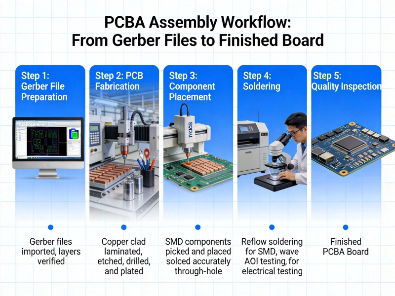
Understanding the PCBA Workflow: From Gerber Files to Finished BoardJune/16/2026
Handling Mixed Technology: Integrating SMT, THT, and Odd-form ComponentsAugust/12/2026

Prototyping vs. Production Assembly: Different Approaches for Different StagesSeptember/08/2026

Challenges in Manufacturing High Aspect Ratio Multilayer BoardsSeptember/07/2026

The Importance of BOM Accuracy in the PCB Assembly ProcessJuly/13/2026

Managing Cost and Quality in Quick Turn PCBsJune/04/2026

Turnkey Assembly: How to Hand Off Your Project and Get Finished ProductsJuly/22/2026