Open Nav

Complex HDI boards push the limits of Pcb Manufacturing. With microblind vias, dense routing, thin dielectrics, and a proliferation of BGA packages at 0.4 mm pitch and finer, these boards carry more electrical and mechanical risk per square centimeter than almost any other class of Electronic Assembly. A failure in the field — whether it manifests as a cracked Microvia, a delaminated buildup layer, or an opens under a BGA — is not a minor inconvenience. In medical, aerospace, and industrial applications, it can be a safety-critical event.
That is why reliability testing is not optional for complex HDI boards — it is an integral part of the design and production validation process. This article covers the specific failure mechanisms in HDI structures, the test methods that detect them, how to design a test plan appropriate to your application, and what the results actually tell you about field performance.
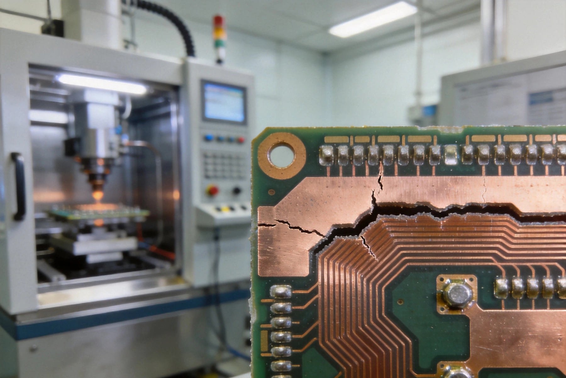
Before reviewing test methods, it helps to understand what can actually fail in an HDI board and why. Standard through-hole Multilayer Boards fail predominantly through barrel cracking at the barrel-to-pad interface and through plating void-induced opens. HDI boards share some of these failure modes, but they also have failure mechanisms that are specific to or amplified by their structure.
The Microvia is the defining feature of HDI, and it is also its most vulnerable element. A microvia barrel is essentially a thin copper tube connecting two adjacent layers. Under thermal cycling, the copper barrel expands and contracts at a different rate than the surrounding dielectric material. Over thousands of thermal cycles, this CTE mismatch creates fatigue damage in the copper barrel, particularly at the barrel-to-pad interface where the stress concentration is highest.
The failure mode is typically an intermittent open — the connection passes at room temperature but fails when the board is at temperature extremes. This makes intermittent microvia opens notoriously difficult to detect with standard continuity testing and explains why thermal cycling is the primary reliability test for microvia integrity.
Sequential lamination builds up the board layer by layer, with each cycle of heat and pressure creating an interface between the new dielectric and the underlying copper or Prepreg. If the surface preparation before lamination is inadequate — insufficient desmear, contamination from handling, or improper oxide treatment — the bond strength at these interfaces will be lower than designed. Under thermal or mechanical stress, delamination can propagate along the interface between buildup layers.
Delamination is a catastrophic failure mode in HDI boards because it can propagate across a significant portion of the board once initiated. Unlike a cracked via, which affects one net, a delamination event can cause multiple nets to fail simultaneously or can cause the board to swell and fail during reflow assembly.
CAF is an electrochemical migration phenomenon in which copper dissolves at the anode (a signal trace under voltage bias) and redeposits as a conductive filament along the glass fiber bundle of the PCB substrate. In standard PCBs, CAF forms along through-hole barrel walls, creating a leakage path or short between adjacent signal layers. In HDI boards, the risk shifts to the thin dielectric between microvia pads and adjacent traces, where the electric field intensity and the proximity of conductors are both higher due to the dense routing.
CAF growth is accelerated by high humidity, high temperature, and voltage bias. For boards deployed in warm, humid environments — outdoor enclosures, industrial process areas — CAF risk must be explicitly evaluated and tested.
As BGA packages get smaller and the pad pitch tighter, the mechanical integrity of the pad structure on the PCB becomes increasingly important. Pad cratering is a fracture in the laminate material beneath the solder pad, typically caused by mechanical shock or thermal cycling. The crack is often invisible under optical inspection and can cause intermittent electrical failures under vibration or thermal stress.
In HDI boards, the buildup dielectric layers under BGA pads are often thin, which means the pad structure has less mechanical backing than in a standard multilayer. Proper pad design — including the use of Via-in-pad plugging and reinforced pad structures — and appropriate testing for pad adhesion and crater resistance are important for boards that will see mechanical shock or vibration in service.
Thermal cycling is the most fundamental reliability test for HDI boards. The board is placed in a chamber that cycles between a high temperature and a low temperature at a defined ramp rate and dwell time. Each cycle exposes the board to the full CTE mismatch stress between copper and dielectric. The number of cycles to failure — or the number of cycles survived before the test is stopped — is the primary output.
For most industrial and commercial HDI applications, a thermal cycling range of -40 to +125 degrees Celsius with 500 to 1,000 cycles is a common test condition. Aerospace and automotive applications may require testing to -55 or even -65 degrees Celsius on the cold end, reflecting the lower temperature extremes encountered in those environments.
The critical metric during TCT is not just whether the board passes — it is whether the electrical resistance of the tested nets increases over the course of the test. A microvia that shows a gradual resistance increase over hundreds of cycles is exhibiting fatigue damage even if it has not yet failed completely. This resistance drift is often the earliest warning sign of an impending failure and is a stronger indicator of long-term reliability than a simple pass/fail criterion.
THB testing exposes the board to high temperature and high humidity while maintaining a voltage bias on selected nets. This test is specifically designed to accelerate CAF formation and to evaluate the board's resistance to moisture ingress. Standard conditions are 85 degrees Celsius and 85 percent relative humidity (often called 85/85 testing), with a bias voltage applied to the nets under test.
For HDI boards used in outdoor or industrial environments, THB testing is particularly important because the thin dielectrics used in HDI buildup layers offer less inherent moisture resistance than the thicker Prepreg layers in standard multilayers. The test duration is typically 1,000 to 2,000 hours, with electrical resistance measurements at regular intervals.
IST is a rapid electrical test method that uses built-in test structures on the PCB to apply controlled thermal stress to the board and measure the change in resistance of the test structures in real time. Unlike thermal cycling, which applies a uniform temperature range to the whole board, IST heats the board from within by passing current through the test structure heaters.
The primary advantage of IST over conventional TCT is speed — IST can complete hundreds of equivalent thermal cycles in a matter of hours rather than days or weeks. It is particularly useful for production lot qualification, where the goal is to verify that a given manufacturing lot of boards meets the reliability standard without spending weeks in a thermal chamber.
IST test structures are designed into the PCB artwork specifically for this purpose. They incorporate representative via structures, trace geometries, and layer transitions that mirror the actual product circuitry. When an IST test structure fails, it provides a direct correlation to how the production circuitry would perform under the same stress conditions.
While thermal cycling uses gradual ramp rates between temperature extremes, thermal shock testing moves the board abruptly from one temperature to another — typically using a two-chamber system where the board is transferred manually or by a mechanical shuttle. The rapid temperature change creates higher stress rates than conventional TCT and is more effective at detecting defects like voids in plating, inadequate interfacial adhesion, and weak solder joints.
Thermal shock is particularly relevant for HDI boards that will experience sudden temperature transients in service — for example, boards in aerospace applications where rapid altitude changes produce sharp temperature swings, or in automotive under-hood environments where a cold engine compartment is rapidly heated on startup.
For HDI boards that will be deployed in portable devices, wearable electronics, or any application where mechanical shock or continuous vibration is expected, drop shock and vibration testing are essential. These tests evaluate the board's ability to withstand mechanical stress without cracking components, delaminating layers, or developing intermittent opens.
Drop shock testing typically uses a half-sine or sawtooth acceleration pulse of defined peak g and duration. Vibration testing uses sinusoidal or random vibration profiles across a frequency range that covers the board's mechanical resonance frequencies. The specific test levels and profiles are defined in standards such as IPC-9701 for board-level drop test methods and MIL-STD-810 for environmental engineering requirements.
Electrical Testing tells you whether a failure occurred. Cross-section analysis tells you where and why it occurred. When a reliability test reveals a failure — whether during accelerated life testing or in a field return — a cross-sectional analysis of the failed area is the definitive diagnostic tool.
In cross-section analysis, the board is potted in an epoxy compound, then ground down to expose the plane of interest, polished, and examined under a microscope at magnification of typically 100x to 500x. This allows the analyst to examine the internal structure of the board — via barrel plating quality, dielectric uniformity, delamination at layer interfaces, and crack propagation paths.
For HDI boards, cross-section analysis requires a skilled laboratory with experience in fine-feature multilayer sectioning. The microvia structures are small enough that poor sectioning technique — uneven grinding, rounding of edges during polishing, or excessive heat from the potting compound — can introduce artifacts that make the analysis inconclusive. Choosing a manufacturer or test lab with documented HDI cross-section experience is important for boards where the reliability data will be used to qualify the design for production.
Cross-section analysis is destructive — the board is consumed in the process. For production qualification or in-process inspection, non-destructive analysis methods are preferred.
X-ray Inspection can reveal internal voids in microvia plating, misalignment between layers, and cracks in buried via barrels without damaging the board. For HDI boards with complex internal structures, 2D X-ray may not provide sufficient resolution, but 3D CT X-ray imaging can generate detailed volumetric reconstructions of the internal board structure.
Scanning Acoustic Microscopy (SAM) is the primary non-destructive tool for detecting delamination and voids in the dielectric layers. A SAM instrument uses ultrasonic pulses that are reflected at internal interfaces — any delamination or void creates a distinctive reflection pattern that can be mapped across the entire board. SAM is particularly valuable for inspecting HDI boards after thermal stress or after rework, where the heat exposure may have caused latent delamination.
Not every HDI board needs every test in this article. The right test plan depends on the board's application environment, the expected product lifetime, the consequence of failure, and the qualification requirements of the target market.
For HDI boards in industrial controllers, factory Automation equipment, and commercial electronics, a baseline qualification package typically includes thermal cycling (500 cycles at -40 to +125 degrees Celsius), IST for lot-to-lot verification, and cross-section analysis of the first article. If the board will operate in uncontrolled indoor environments, THB testing should be added to evaluate moisture resistance. Vibration testing is added if the board will be deployed in a motor-driven or rotating machine environment.
Automotive Hdi boards must meet AEC-Q100 or AEC-Q200 qualification standards depending on the component type, and the PCB-level qualification is typically defined in AEC-Q100 in combination with the OEM-specific qualification specifications. The test conditions are more aggressive than commercial equivalents — wider temperature range, higher cycle counts — and the test-to-failure data must be statistically significant, not just based on a single test vehicle.
Medical device PCB qualification follows the design controls requirements of the applicable regulatory framework — FDA 21 CFR Part 820 in the United States, the EU Medical Device Regulation (MDR) in Europe, or the equivalent in other jurisdictions. The reliability testing plan is typically defined during the design and development phase and validated against the intended use environment of the device. For implantable or body-worn medical devices, the temperature and humidity exposure conditions are augmented by mechanical flex testing for boards that will be subject to body movement stress.
Defense and aerospace electronics follow MIL-PRF-31032 or MIL-PRF-55110 for PCB qualification, with environmental test requirements defined in MIL-STD-810. The test plans for HDI boards in these applications are the most demanding in terms of thermal extremes, vibration levels, and the statistical rigor of the test population. Extended thermal cycling (1,000 to 2,000 cycles), combined thermal-vibration testing, and radiation hardness evaluation for space applications are all within scope for the most demanding programs.
Reliability test results require careful interpretation. A board that passes 1,000 thermal cycles does not guarantee a 20-year field life. It guarantees that the board survived 1,000 cycles at the test conditions — which may or may not be representative of the actual field conditions. The correlation between accelerated life test results and field performance depends on how well the acceleration factors for each failure mechanism are understood and how accurately the test conditions represent the field environment.
Microvia fatigue has a relatively well-characterized acceleration factor: approximately 2x the failure rate for every 10 degrees Celsius increase in the average cyclic temperature. This allows engineers to use thermal cycling data to project field life with reasonable confidence, provided the test temperature range is representative of the actual field temperature range.
CAF formation has a more complex acceleration relationship that involves temperature, humidity, voltage, and time. Projecting field life from THB test data requires careful modeling and should be done in consultation with the Pcb Manufacturer or a qualified reliability engineering consultant.
Most importantly, reliability test results are specific to the manufacturing lot represented by the test vehicles. A board that passes qualification testing does not guarantee that the next production lot — with different laminate批次, different plating bath chemistry, or different lamination parameters — will perform identically. Ongoing lot qualification testing and statistical process control on key fabrication parameters are the practical tools for maintaining reliability consistency across production lots.
Complex HDI boards present unique reliability challenges that cannot be addressed by testing alone — but testing done right provides the evidence that a design is fit for its intended purpose and that a manufacturing lot meets the quality standard established during qualification.
The most effective reliability program for HDI boards combines accelerated life testing (thermal cycling, THB, thermal shock), non-destructive inspection (X-ray, acoustic microscopy), and destructive physical analysis (cross-section) as complementary tools, not substitutes for each other. Each method reveals different information about the board's integrity.
Designing a test plan that is proportionate to the application — not over-testing simple boards or under-testing safety-critical ones — is the engineering judgment that experienced HDI manufacturers and reliability engineers bring to the process. That judgment, informed by failure mode knowledge and supported by test data, is what separates a qualification program that provides genuine confidence from one that merely checks a compliance box.
Contact us to discuss your requirements.

Inventory Management and Kitting: Streamlining Your Supply Chain with PCB ServicesJuly/15/2026
How to Find the Right PCB Fabrication Partner in ChinaJune/02/2026
8-Layer vs. 16-Layer: Deciding on the Right Stack-up for Your Multilayer BoardJune/08/2026
Managing Signal Integrity and Impedance Control in High-Speed Multilayer PCBsJuly/21/2026
The Benefits of Combining PCB Fabrication and AssemblyMay/22/2026

From Prototype to Mass Production: Scaling Your Custom PCB Project SeamlesslyJuly/07/2026
Exploring Special Materials in Custom PCB FabricationMay/21/2026

How AI-Driven Scheduling is Making Rapid PCB Prototyping More ReliableJune/18/2026