Open Nav

The global Pcb Manufacturing industry stands at the precipice of its most transformative era. Driven by AI server proliferation, 800G/1.6T optical module deployment, automotive electrification, and the relentless push toward higher integration, PCB mills that once competed primarily on cost and throughput are now being redefined by a new suite of capabilities. Future-proofing is no longer a strategic luxury—it is an operational imperative. This article examines the emerging capabilities that will separate tomorrow’s leading PCB mills from yesterday’s incumbents.
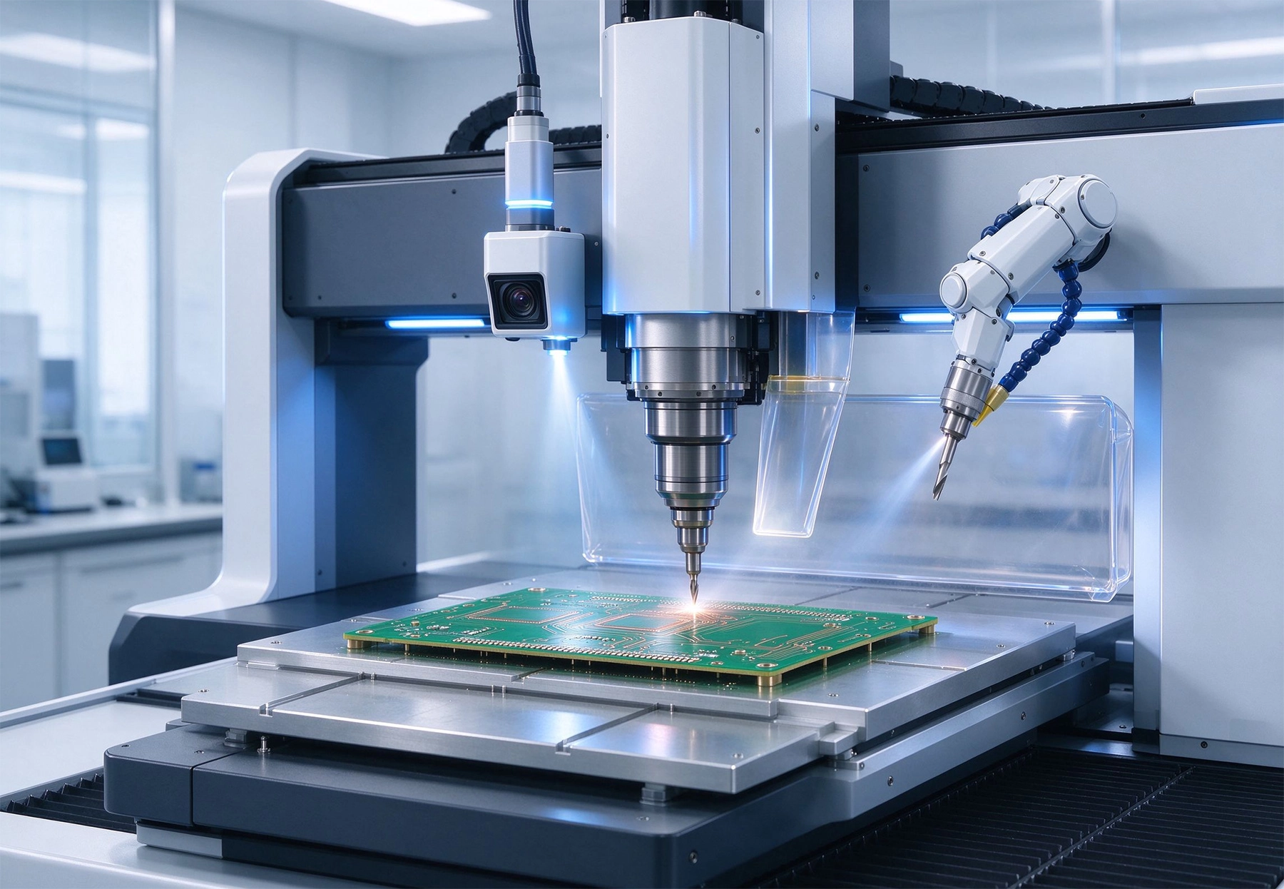
Artificial intelligence is moving from pilot projects to production-line backbone in forward-looking PCB mills. Deep-learning-based Aoi (Automated Optical Inspection) systems now achieve defect identification rates approaching 99% while dramatically reducing false-call rates that plagued first-generation rule-based inspectors. By training on thousands of labeled defect samples—shorts, opens, copper roughness, pinholes, solder bridges—these systems classify defect types autonomously and trace them back to specific process steps, turning quality data into actionable process intelligence.
Beyond inspection, AI-driven process optimization continuously tunes plating, etching, and lamination parameters by ingesting real-time sensor data—temperature, speed, current, pressure—from hundreds of points across the line. The result is stabilized yield curves and reduced chemical and energy consumption. Predictive maintenance, powered by time-series models analyzing drill wear, exposure tool degradation, and plating bath chemistry, shifts equipment management from reactive repair to proactive intervention, cutting unplanned downtime that has historically eroded OEE in multi-variety production environments.
At the planning layer, AI integrated with MES (Manufacturing Execution Systems) orchestrates intelligent scheduling across order books, material availability, machine states, and labor shifts—critical for mills serving the growing HMLV (High-Mix Low-Volume) segment where changeovers can occur multiple times per day.
The convergence of AI server architecture and next-generation optical interconnects is pushing PCB feature sizes into territory that demands fundamentally new tooling. mSAP (Modified Semi-Additive Process) has emerged as the dominant pathway for achieving line widths and spacings below 15 micrometers—a requirement driven by 1.6T optical modules and advanced packaging architectures like CoWoP. Unlike traditional subtractive methods, mSAP employs ultra-thin seed copper layers, pattern plating, and flash etching to produce steep sidewall profiles and precise width control, enabling high-density routing with low signal loss.
Ultrafast Laser Drilling is replacing conventional mechanical drilling in high-mix environments where Microvia density and aspect ratio demands exceed the practical limits of carbide bits. Femtosecond and picosecond lasers ablate material with minimal heat-affected zones, preserving dielectric integrity—particularly critical when processing next-generation low-loss substrates such as M9-grade resins. As via density increases and via diameter shrinks, ultrafast laser drillers are seeing both volume and value acceleration, with some suppliers reporting lead times extending well into 2027.
LDI (Laser Direct Imaging) equipment has become the exposure standard for high-density PCBs, offering micrometer-level resolution and registration accuracy that phototool-based systems cannot match. Modern LDI tools with dual-side alignment and real-time overlay correction enable consistent patterning on multi-layer stacks where cumulative registration errors have historically plagued yield.
Material science is no longer a passive input—it is an active differentiator. Ultra-low Dk/Df resins (M9 and beyond), PTFE-based laminates, and quartz fabric reinforcements are becoming table stakes for boards serving 800G and 1.6T switch fabrics. These materials reduce signal transmission loss significantly, but they impose stricter requirements on drilling chemistry, copper roughness control, and lamination cycle profiles. PCB mills that develop in-house material qualification capabilities—ability to co-develop substrate specifications with CCL vendors—gain a formidable moat.
High-velocity low-profile (HVLP) copper foils and ultra-thin copper foils are now essential for preserving Signal Integrity at multi-lane speeds exceeding 56 Gbps. The ability to manage copper roughness specifications across multiple substrate suppliers while maintaining consistent ESR (Equivalent Series Resistance) performance is becoming a key competency that separates premium mills from commodity producers.
Meanwhile, embedded component technology—placing passive and active components directly within the PCB substrate—is transitioning from niche application to mainstream strategy. Chip-on-Substrate approaches eliminate discrete heat spreaders, reduce system footprint, and improve thermal performance. Though requiring semiconductor-grade cleanroom environments and precision placement equipment, this capability is already finding adoption in high-power density modules and is poised for broader diffusion as equipment costs decline.
The most future-ready PCB mills are building digital twin capabilities that simulate entire fabrication sequences before a single panel enters the line. AI-accelerated electromagnetic simulation replaces brute-force FEM solvers, enabling rapid SI/PI (Signal Integrity/Power Integrity) analysis and thermal hotspot identification during the design phase. Generative AI assistants integrated with EDA tools autonomously propose routing solutions that optimize Impedance Control, crosstalk mitigation, and thermal dissipation—cutting board design cycles by 40% or more for complex multi-layer server PCBs.
AI-Dfm (Design For Manufacturability) engines parse Gerber and ODB++ files to preemptively flag width/spacing violations, drill interference, plating risk zones, and lamination warpage potential—catching manufacturability issues before tape-out rather than during first-article inspection. This shift-left approach reduces Prototype iteration counts and accelerates time-to-volume, a critical advantage in markets where architectural changes between silicon revisions are common.
Environmental compliance is transitioning from a cost center to a market differentiator. Next-generation PCB mills are deploying closed-loop chemical recovery systems, zero-liquid-discharge plating circuits, and AI-optimized energy management that dynamically adjusts HVAC, chiller, and exhaust systems to real-time production loads. For export-oriented mills serving EU and North American OEMs with Scope 3 emissions reporting requirements, verifiable green manufacturing credentials are becoming a procurement prerequisite—not a nice-to-have.
Lead-free Solderability preservation, halogen-free laminate handling, and water-stewardship metrics are now embedded in quality scorecards. Mills that can demonstrate quantified reductions in chemical consumption per square meter and carbon intensity per shipped panel will command price premiums and access to Sustainability-linked procurement programs.
The post-pandemic era has rewritten the rules of Supply Chain management for PCB manufacturers. Geopolitical fragmentation, raw material volatility, and customer demands for shorter lead times have converged to make agility a core competency. Leading mills are building multi-tier supplier visibility platforms that track raw material inventory, substitute material qualification status, and alternate source readiness in real time.
HMLV production capability—the ability to economically produce small batches of diverse products with rapid changeover—has moved from niche to mainstream. SMED (Single-Minute Exchange of Die) methodologies, modular workstations, and flexible Automation allow changeovers in under 30 minutes—a stark contrast to the 24-hour changeover times that plagued conventional lines. This flexibility, combined with digital work instruction systems that auto-configure equipment parameters per job recipe, enables mills to serve Prototype-to-production customers who value speed and adaptability over pure unit cost.
The blurring boundary between Pcb Manufacturing and semiconductor packaging is creating new capability frontiers. Advanced packaging architectures like CoWoP (Chip-on-Wafer-on-Printed board) and NPO (No-Substrate-Parasitic-Optics) are driving demand for PCB-like substrates with semiconductor-grade flatness and dimensional stability. Mills that invest in CMP (Chemical Mechanical Polishing) integration, ultra-precise thinning processes, and semiconductor-grade cleanroom environments position themselves to capture value from this convergence trend.
Similarly, the push toward silicon photonics integration and optical interconnects on PCB substrates is creating demand for precision micro-machining capabilities previously confined to foundry environments. Mills that develop hybrid mechanical-optical processing lines—combining laser structuring, precision dicing, and optical alignment—will be uniquely positioned to serve the growing market for optical I/O modules in AI inference clusters.
The next generation of PCB mills will not compete on price alone. Their competitive architecture will be built on five pillars: AI-driven intelligence that turns data into yield, ultra-precision tooling that unlocks new design freedoms, materials expertise that co-evolves with substrate innovation, digital twin capabilities that compress development cycles, and sustainable operations that meet the ESG demands of global OEMs. Mills that invest strategically across these dimensions today will be the ones defining the industry’s trajectory tomorrow. For PCB manufacturers, future-proofing is not about predicting the exact technology of tomorrow—it is about building an adaptive, data-rich, and agile manufacturing organism capable of evolving with whatever comes next.
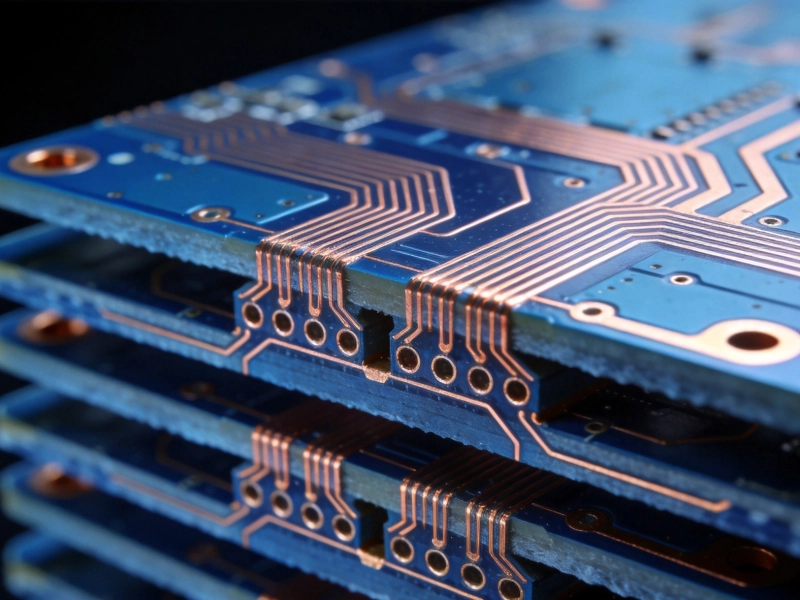
Cost Drivers in HDI and Multilayer PCB Fabrication: What Engineers Need to KnowSeptember/26/2026
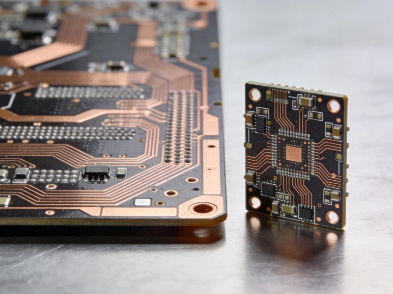
Large Format vs. Miniature PCBs: Evaluating Size Constraints and CapacitiesAugust/14/2026

Minimum Trace and Space: How Far Has PCB Technology Advanced?July/01/2026
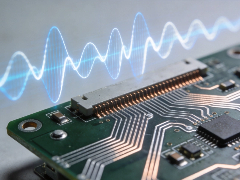
High-Frequency Materials: Assessing Capabilities for RF and Microwave PCBsJuly/23/2026
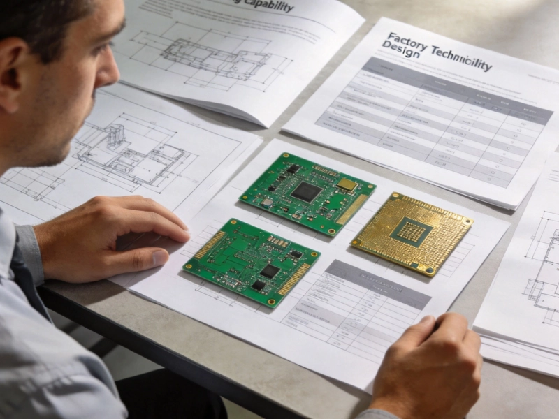
Why Capability Statements Matter: Matching Your Design Needs to Factory StrengthsOctober/09/2026
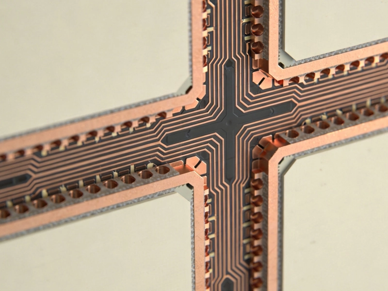
Any-Layer Interconnect: The Pinnacle of High-Density PCB TechnologyJuly/10/2026
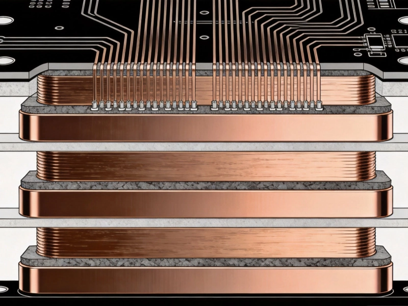
Heavy Copper PCBs: Capabilities for High-Current and Power ElectronicsJuly/14/2026
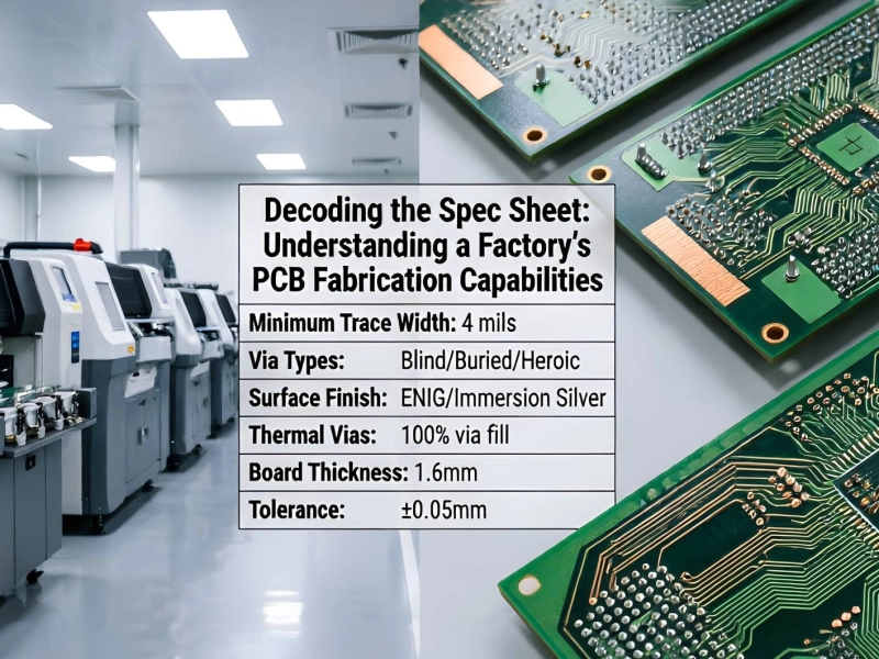
Decoding the Spec Sheet: Understanding a Factory's PCB Fabrication CapabilitiesJune/11/2026