Open Nav

There is a lot of talk about Sourcing Pcbs From China. Some of it is hype. Some of it is horror stories. Most of it misses the point. The reality of how Chinese PCB factories actually work is less dramatic than either the enthusiasts or the skeptics claim. It's a complex, functional Supply Chain with real advantages and real challenges—and understanding how it operates gives you a massive edge whether you're ordering 10 prototypes or 10,000 production boards.
This article strips away the marketing language and gives you the ground-level view of how Chinese Pcb Manufacturing actually functions.
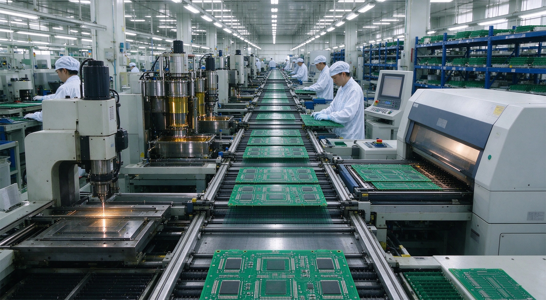
China dominates global Pcb Production for one simple reason: it built an ecosystem. Not just factories, but the entire supporting infrastructure—laminate suppliers, drill bit manufacturers, chemical processors, logistics companies, and the people who know how to run them all. This didn't happen overnight. The Chinese PCB industry took decades to mature, accelerating rapidly after the early 2000s when major OEMs began shifting production to take advantage of lower costs and available capacity.
Today, the industry is stratified. At the top are large manufacturers serving consumer electronics giants—companies that produce millions of boards per month for smartphones, laptops, and automotive electronics. These fabs are highly automated, extremely efficient at high volume, and largely inaccessible to small and medium buyers. They have minimum orders that would tie up most startups' capital for quarters.
Below them is a vast middle tier: factories that serve the global market for low to mid-volume production. These are the shops most international buyers actually work with. They range from operations with a few hundred employees running aging but well-maintained equipment to modern facilities with impressive Automation and quality systems. The gap between the best and the rest in this tier is enormous—due diligence matters enormously here.
When you submit a PCB order to a Chinese manufacturer, you're often not dealing directly with the factory floor. The Supply Chain has layers that surprise many first-time buyers:
The key insight: the factory that actually makes your board may be different from the company you place the order with. For prototypes and small batches, this is usually fine. For production orders where consistency matters, understanding the actual manufacturing path becomes important.
A PCB doesn't emerge from a single machine. It passes through a sequence of specialized processes, most of which are performed by different shops or departments within a larger facility. Here's what actually happens:
The process starts with laminate—copper-clad substrate material. Most Chinese factories source their laminates from major suppliers like Shengyi, Kingboard, or Iteq, all of which produce quality materials at competitive prices. The copper thickness, material type (FR-4, high-Tg, Rogers, etc.), and panel size are determined by your specifications.
Once the panel is cut to size, the inner layer pattern is imaged using Photoresist and UV exposure. For complex boards, this involves multiple imaging steps with registration tolerance measured in microns. Chinese factories have invested heavily in imaging equipment—laser direct imaging (LDI) systems are now common even in mid-tier shops, dramatically improving fine-line capability.
After imaging, copper is etched away to form the inner layer traces. The accuracy of this step determines whether your fine-pitch components will actually solder correctly. Registration—how precisely the inner layers align with each other and with the outer layers—becomes increasingly critical as feature sizes shrink.
Chinese factories that serve the international market have gotten quite good at registration. Tolerance of ±0.05mm on layer-to-layer alignment is standard among competent shops. If you need tighter tolerance, you pay more and need to specify clearly.
Inner layers are aligned, prepregs (bonding sheets) are stacked, and the panel is laminated under heat and pressure. This step bonds the layers together into a solid core. Then the through-holes are drilled—CNC drilling with carbide or diamond-coated bits. Drill quality and accuracy vary significantly between shops. Entry-level factories may use older equipment that struggles with small holes or tight tolerances.
The drilled holes are plated with copper to create the via barrels. This involves a series of chemical baths—desmear, activation, copper plating, and sometimes tin-lead or Enig (electroless nickel immersion gold) surface finish. The plating process is where defects like voids, notches, or thin spots can occur, particularly on boards with high aspect ratio holes (deep holes relative to their diameter).
Outer layers are then patterned using the same imaging and Etching Process as inner layers. For boards with buried or Blind Vias, additional steps are inserted here—each via type requires its own lamination-drill-plate sequence.
Surface finish options significantly impact cost and lead time. Hasl (hot air solder leveling) is the cheapest option but offers uneven coverage on fine-pitch components. Enig provides flat surfaces ideal for BGA and fine-pitch work but costs more. Lead-free Hasl has largely replaced tin-lead in commercial production due to RoHS requirements.
Solder Mask—typically green, though other colors are available—is applied over the base laminate except at pad locations. The quality of Solder Mask application varies: high-end factories use pneumatic spray coating for consistent coverage; lower-cost shops may use screen printing that leaves thickness variation, particularly around fine features.
Before shipping, boards are tested for continuity and isolation. Flying Probe testing is common for low to medium volumes—it's flexible and doesn't require custom tooling. For high volumes, fixture-based in-circuit test provides faster throughput but requires upfront fixture cost.
Visual inspection is performed manually or with automated optical inspection (Aoi) systems. Aoi catches obvious defects like shorts, opens, and missing components on assembled boards but may miss buried defects. For critical applications, X-ray Inspection or microsection analysis may be specified—this adds significant cost but provides certainty about internal quality.
Understanding why Chinese factories can offer competitive pricing helps you negotiate better and set realistic expectations:
A factory running three shifts processing hundreds of panels per day has completely different economics than a shop building ten panels a week. Fixed costs—equipment, floor space, overhead staff—are spread across far more units. Chinese factories serving the global market have optimized for this scale in ways that Western shops cannot easily replicate.
Labor costs in China have risen significantly over the past two decades, but they remain substantially lower than in North America, Europe, or Japan for equivalent skills. This isn't just assembly line workers—it's engineers, quality technicians, and process operators. A factory engineer in Shenzhen might earn one-quarter of their equivalent in Silicon Valley, even while operating more sophisticated equipment.
The Pearl River Delta—particularly Shenzhen and the surrounding cities—has the world's most concentrated PCB supply chain. Laminates, chemicals, drill bits, specialty tools, and logistics services are all available locally within hours. This reduces inventory costs, shipping costs, and lead times. A factory needing a specific material can source it same-day; the same transaction might take a week elsewhere.
Chinese PCB manufacturers have benefited from government support in various forms—land leases, tax treatment, infrastructure investment, and in some cases direct subsidies. Whether you view this as unfair competition or simply acknowledge it as a factor, it does influence pricing structure in the market.
Understanding failure modes helps you prevent them:
Chinese factories are exceptionally good at building to specification. They struggle with ambiguity. If your specification doesn't clearly define acceptable criteria for a parameter, you will get the cheapest interpretation. Clear, detailed fabrication drawings with explicit tolerances prevent most disputes.
English documentation doesn't always translate to clear understanding. Technical terms are misinterpreted, requirements are paraphrased incorrectly when passed from sales to engineering, and critical details are lost. The more complex your board, the more important it is to have direct communication channels with the factory's technical team.
A factory may offer different quality levels at different price points, using different equipment and inspection criteria. The sample you approved may not match production boards if quality verification isn't specified and enforced. Always specify your quality acceptance criteria explicitly—AOI standards, test requirements, acceptable defect rates, and inspection documentation.
For turnkey assembly, component supply chains introduce another layer of risk. Chinese distributors may source from multiple brokers, and component authenticity cannot always be guaranteed. Counterfeit ICs are a known problem in the global Electronics Supply Chain. If component authenticity is critical for your application, source components yourself and use consignment assembly.
The buyers who get the best results from Chinese Manufacturing tend to share certain practices:
Never scale up before validating quality with a small order. Order a Prototype batch, inspect it thoroughly, and only then commit to larger quantities. The cost of a failed production run far exceeds the savings from moving quickly.
Chinese business culture values relationships. A factory that knows you, understands your application, and trusts your consistency will go further to solve problems than one treating you as a one-time transaction. Visit when possible. Communicate regularly. Pay on time.
Your fabrication drawing should be complete enough that the factory could build your board without a single question—and every question they do ask indicates a gap in your specification. Include material specs, tolerance requirements, test requirements, inspection criteria, and packaging instructions. The more explicit you are, the less ambiguity you leave for interpretation.
Chinese factories operate at high utilization. Lead times fluctuate with demand. Standard lead times of 5 to 10 working days are common for simple boards, but can stretch to 3 to 4 weeks during peak seasons or for complex boards. Build buffer time into your schedule, particularly for initial orders where you may need iteration.
Sea freight is cheap but slow—3 to 6 weeks from Shenzhen to US West Coast. Air freight is faster but expensive. Express couriers like DHL and FedEx offer reasonable middle-ground for samples and small batches but become prohibitively expensive for larger orders. Plan your logistics as part of your manufacturing schedule, not as an afterthought.
The landscape is shifting. Rising labor costs, environmental regulations, and geopolitical tensions are all reshaping the industry:
The cost advantage of Chinese Manufacturing will persist but narrow. For buyers, the strategic advantage shifts from pure cost arbitrage to relationship building, Quality Assurance, and supply chain resilience.
Chinese PCB factories are not magic. They're industrial operations with strengths, weaknesses, and business incentives like any other manufacturer. The buyers who succeed treat them as partners rather than commodities, invest in clear communication, and maintain the same quality discipline they'd apply to domestic suppliers.
The supply chain is real and mature. It's also evolving. Understanding how it actually works gives you the foundation to make smart sourcing decisions—not just for today's project, but for the supply chain strategy you'll need as your products scale.
Sourcing from China is safe if you work with reputable manufacturers and verify their capabilities before committing. Many Chinese factories meet or exceed international quality standards. The risks are the same as any supplier relationship: unclear specifications, quality inconsistency, and communication gaps. Proper due diligence and clear documentation mitigate these risks significantly.
Start with industry directories, trade show connections (like productronica or IPC shows), and referrals from other engineers. Request samples before large orders, verify their quality management system (ISO 9001 is a baseline), and check references. Online platforms with review systems can provide useful feedback from other buyers. For critical applications, consider third-party inspection services.
Standard lead times range from 5 to 15 working days for simple boards, depending on the manufacturer and order volume. Complex boards with advanced specifications may require 15 to 30 working days. Shipping adds 3 to 6 weeks for sea freight or 5 to 10 days for air freight. Plan for potential delays during Chinese holidays and peak manufacturing seasons.
PCB costs from Chinese manufacturers are typically 30% to 70% lower than equivalent boards from Western manufacturers, depending on complexity, quality level, and order volume. The savings are most significant for high-volume, standard-specification boards. Complex boards with advanced materials or tight tolerances see smaller differentials because the specialized capabilities are rarer and more evenly distributed globally.
Yes. Many Chinese manufacturers and online platforms specifically serve the Prototype market with minimum orders as low as 5 boards or even 1 board. These services are designed for engineers validating designs, not just for production scale-up. Quality varies, so due diligence still applies, but low minimums are widely available.
Contact us to discuss your requirements.
High-Frequency Materials: Assessing Capabilities for RF and Microwave PCBsAugust/03/2026
Large Format vs. Miniature PCBs: Evaluating Size Constraints and CapacitiesAugust/14/2026
Any-Layer Interconnect: The Pinnacle of High-Density PCB TechnologyJuly/10/2026
Why Global Brands Are Turning to PCB Fabrication in China in 2026May/21/2026
Back-drilling and Via-in-Pad: Advanced Capabilities for High-Speed DesignsSeptember/29/2026
The Role of Equipment in Determining PCB Fabrication Capabilities (LDI, Laser Direct Imaging)September/09/2026
Heavy Copper PCBs: Capabilities for High-Current and Power ElectronicsJuly/14/2026
Future-Proofing: Emerging Capabilities in the Next Generation of PCB MillsOctober/12/2026