Open Nav

Every electronic device you use, from your smartphone to your car's engine control unit, relies on a Printed Circuit Board (PCB). For beginners entering the world of electronics, the journey from a circuit diagram to a fully functional board can seem daunting. However, understanding the fundamental stages of PCB Fabrication and Assembly: A Step-by-Step Guide for Beginners is the key to bridging the gap between design and a working product.
In this comprehensive guide, I will walk you through the entire lifecycle of a PCB. We will explore how bare boards are manufactured (fabrication) and how electronic components are attached to them (assembly). Whether you are a hobbyist looking to build your first project or a student aiming to understand manufacturing processes, this article will provide the clarity you need.
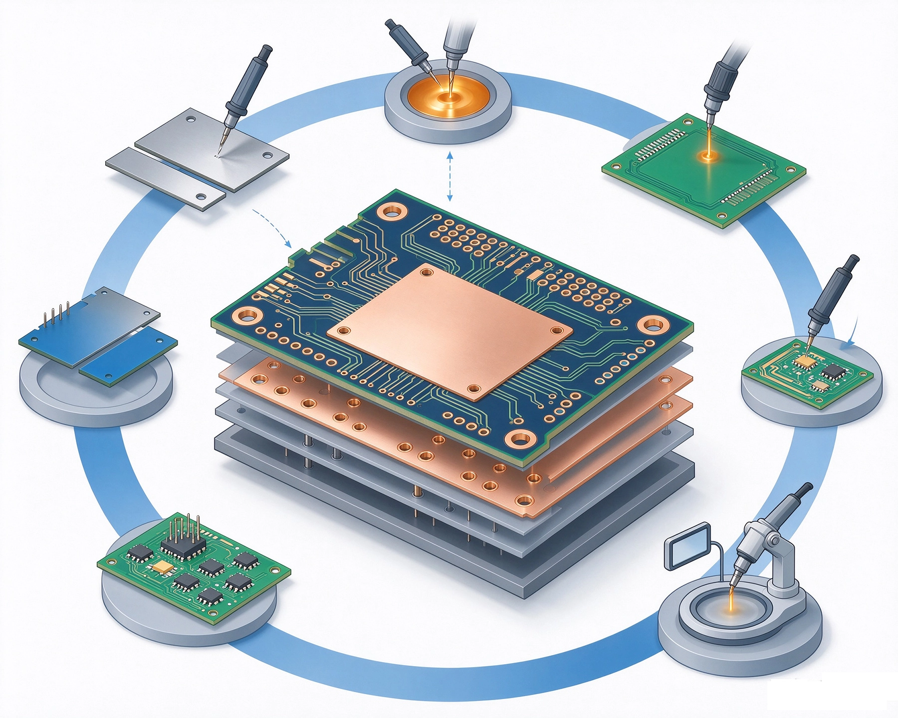
Fabrication is the process of creating the physical structure of the circuit board. This involves turning your digital design files (Gerber Files) into a physical board with copper traces, holes, and a protective coating.
Everything starts with the design. Engineers use CAD software to layout the circuit. Once finished, the design is exported as Gerber Files. These files act as the "blueprint" for the manufacturer. The first physical step is printing these designs onto a transparent film using a plotter printer. Each layer of the PCB (inner layers, outer layers, Solder Mask) gets its own film.
The core of a standard PCB is a substrate, typically made of FR-4, a glass-reinforced epoxy laminate. This substrate is clad with copper on both sides. To create the Circuit Pattern:
This is the most critical chemical step. The board is washed in an alkaline solution to remove the unhardened photoresist, exposing the unwanted copper. It is then submerged in a chemical etchant (often ammoniacal etching or Cupric Chloride) which eats away the exposed copper. Only the copper protected by the hardened photoresist remains. Finally, the remaining photoresist is stripped off, leaving behind the clean copper Circuit Pattern.
For multi-layer boards, the inner layers are aligned and "sandwiched" with sheets of Prepreg (adhesive) and copper foil. This stack is heated and pressed in a hydraulic press to fuse them into a single unit. Once laminated, an X-ray machine locates the registration points, and a drill creates holes for vias and through-hole component leads. Precision here is vital; a misaligned drill can sever connections.
Before the board is usable, it needs protection. A Solder Mask (usually green ink) is applied to cover the copper traces, preventing oxidation and accidental short circuits. Finally, a surface finish like Hasl (Hot Air Solder Leveling) or Enig (Electroless Nickel Immersion Gold) is applied to the exposed pads to ensure they are solderable. Understanding these basics of PCB Fabrication and Assembly: A Step-by-Step Guide for Beginners helps you appreciate why board quality varies.
Once the bare board is fabricated, it moves to the assembly stage. This is where components are mounted. The two primary technologies are Surface Mount Technology (SMT) and Through-Hole Technology (THT).
Smt Assembly begins with applying solder paste—a mixture of tiny solder balls and flux—to the board. A stainless steel stencil is placed over the PCB, and a squeegee blade pushes the paste across it. The paste is deposited only on the component pads through the stencil openings. This step is crucial; too much paste causes bridging, while too little causes open joints.
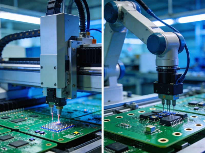
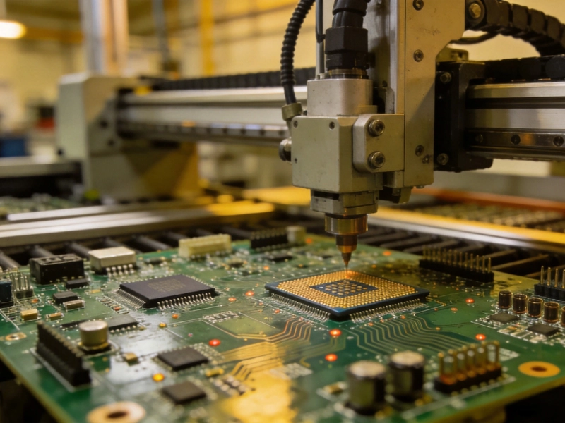
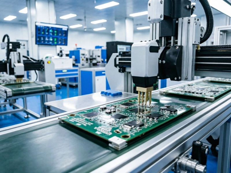
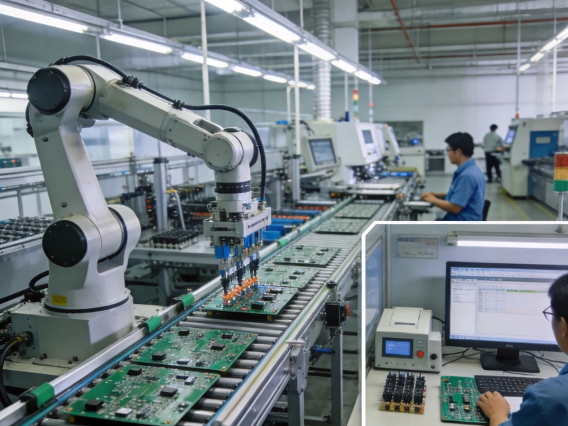
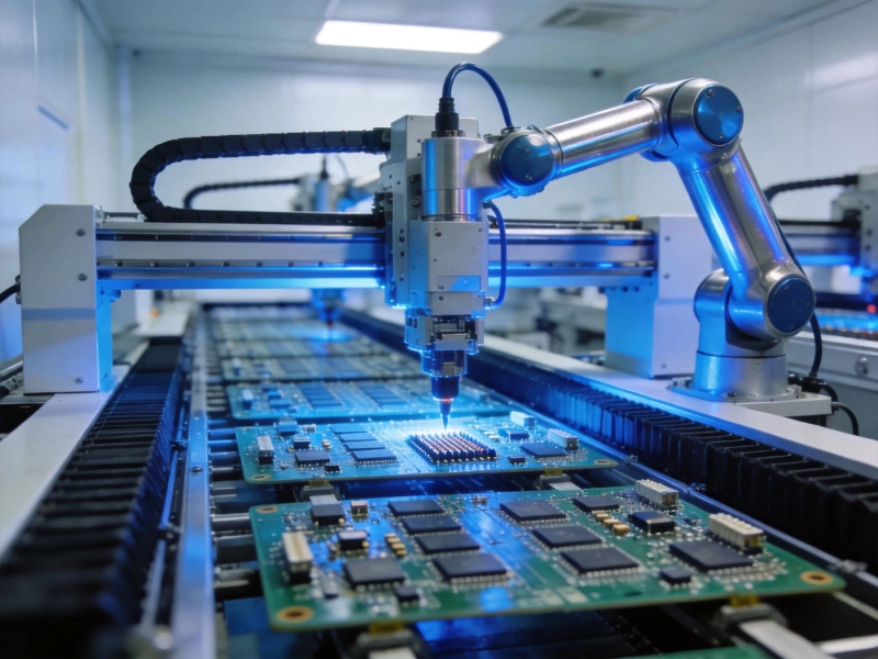
Robotic machines, known as Pick and Place machines, populate the board. These machines use a vacuum nozzle to pick up components from reels or trays and place them onto the solder paste with incredible speed and precision. Modern machines can place tens of thousands of components per hour. This Automation is what makes Pcb Fabrication and Assembly: A Step-by-Step Guide for Beginners scalable for mass production.
Once all components are placed, the board travels through a reflow oven. The oven heats the board according to a specific thermal profile. The solder paste melts (reflows), creating a permanent electrical and mechanical bond between the component leads and the PCB pads. The board then cools, solidifying the joints.
Not all components are Surface Mount. Large connectors or capacitors often use through-hole technology. These components have leads that pass through drilled holes. They are typically soldered using wave soldering, where the board passes over a wave of molten solder, or by hand soldering for low-volume runs.
No manufacturing process is complete without verification. In professional manufacturing, we use Automated Optical Inspection (Aoi) to scan the board for defects like missing components, misalignment, or solder bridges. For complex boards with Ball Grid Arrays (BGAs), X-ray Inspection is used to check the solder joints hidden beneath the component.
Sometimes, the flux residue is not cleaned properly, which can lead to corrosion over time. We must ensure the cleaning process is thorough, especially for high-reliability electronics. A quick visual check by a human operator is also a good practice to catch what machines might miss.
From the chemical etching of copper to the robotic placement of microscopic resistors, the journey of a PCB is a marvel of modern engineering. By understanding the distinct phases of fabrication and assembly, you can make better design decisions and troubleshoot issues more effectively. Mastering the concepts in this Pcb Fabrication and Assembly: A Step-by-Step Guide for Beginners is your first step toward becoming a proficient electronics engineer.
SMT (Surface Mount Technology) involves mounting components directly onto the surface of the PCB, allowing for smaller and denser designs. THT (Through-Hole Technology) involves inserting component leads through holes in the board, offering stronger mechanical bonds but taking up more space.
The solder mask protects the copper traces from oxidation and environmental damage. It also prevents solder bridges from forming between closely spaced solder pads during the assembly process.
Gerber files are the standard vector format used by PCB designers to communicate the board layout to the manufacturer. They define the copper layers, solder mask, Silkscreen, and drill data.

Prototyping vs. Production Assembly: Different Approaches for Different StagesSeptember/08/2026
SMT vs THT PCB Assembly in China: Which Technology is Right for Your Project?June/10/2026
Handling Mixed Technology: Integrating SMT, THT, and Odd-form ComponentsAugust/12/2026
How Chinese Manufacturers Ensure Precision in the SMT PCB Assembly ProcessJune/03/2026
Turnkey Assembly: How to Hand Off Your Project and Get Finished ProductsJuly/22/2026
The Importance of BOM Accuracy in the PCB Assembly ProcessJuly/13/2026
The Benefits of Combining PCB Fabrication and AssemblyMay/22/2026
Inspection Standards: IPC-A-610 and What it Means for Your Assembled BoardsAugust/03/2026