Open Nav

Custom printed circuit boards (PCBs) are the foundation of modern electronic products, from innovative consumer devices to complex industrial equipment. However, designing a Custom Pcb that functions correctly in the lab is only half the challenge—the other half is designing a board that can be manufactured reliably, consistently, and cost-effectively at scale.
This is where Design For Manufacturability (Dfm) comes in. Dfm is the practice of designing products with the manufacturing process in mind, ensuring that the design is compatible with the capabilities of the manufacturing process, minimizing production issues, reducing costs, and improving quality. For Custom Pcb projects, implementing DFM early in the design process is the single most important factor in determining project success, avoiding costly redesigns, production delays, and quality issues.
This guide explores the critical role of DFM in custom board success, its key benefits, core guidelines, common mistakes to avoid, and how to implement DFM effectively in your custom PCB projects.
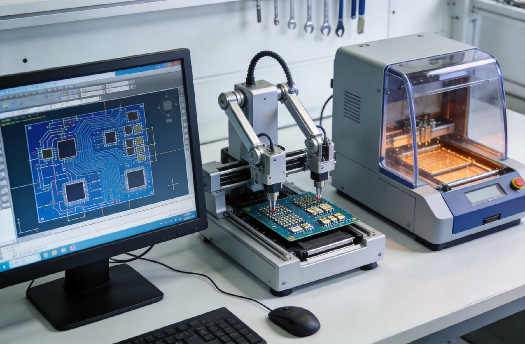
Design For Manufacturability for PCBs is a systematic approach to design that considers the entire manufacturing process from the earliest stages of Product Development. DFM ensures that the Pcb Design can be manufactured efficiently, reliably, and cost-effectively by the chosen Pcb Manufacturer, while still meeting all functional and performance requirements of the product.
Unlike traditional design approaches where the design is completed first and then sent to manufacturing for production, DFM integrates manufacturing considerations into every step of the design process. This includes understanding the capabilities and limitations of Pcb Manufacturing processes, material availability, assembly requirements, testing processes, and yield optimization.
DFM for custom PCBs encompasses several related disciplines:
Effective DFM requires close collaboration between design engineers and manufacturing engineers from the earliest stages of the project, ensuring that design decisions balance performance requirements with Manufacturing Capabilities and cost constraints.
Implementing DFM in your custom PCB project delivers significant benefits across the entire product lifecycle:
DFM can reduce Pcb Manufacturing costs by 20-50% by optimizing the design for efficient production. For example, designing to standard process capabilities instead of requiring specialized or custom processes reduces manufacturing complexity and cost. DFM also reduces scrap rates during production by eliminating design features that are difficult to manufacture and result in low yields. Additionally, DFM can reduce material costs by optimizing layer counts, using standard material sizes, and minimizing waste during manufacturing.
DFM eliminates the need for costly and time-consuming design iterations after the design is sent to manufacturing. Designs that pass Dfm Checks can go directly into production, while designs with DFM violations require redesign, rechecking, and resubmission, adding weeks or even months to the project timeline. DFM also reduces production time by optimizing the design for efficient manufacturing, reducing the number of process steps required.
DFM eliminates design features that are prone to manufacturing defects, resulting in higher quality boards with fewer field failures. For example, designing with sufficient clearances and tolerances reduces the risk of short circuits, open circuits, and solder joint defects. DFM also improves long-term reliability by ensuring the design is robust to manufacturing variations, environmental stress, and wear over time. Products designed with DFM have significantly lower warranty claims and field failure rates compared to products designed without DFM consideration.
Without DFM, it is common for custom PCB projects to require 2-3 or more design iterations before the design can be successfully manufactured. Each iteration costs time and money, delaying product launch and increasing development costs. DFM catches potential manufacturing issues early in the design process when changes are relatively inexpensive and easy to implement, reducing the need for redesigns after Prototype production.
DFM reduces the risk of unexpected production issues, yield problems, and quality issues that can derail a product launch. By validating the design against Manufacturing Capabilities before production begins, you can identify and address potential issues early, eliminating surprises during production. This is especially important for high-volume production runs, where yield issues can result in significant financial losses and product shortages.
Designs created with DFM are easier to scale from Prototype production to mass production. DFM ensures that the design is compatible with high-volume manufacturing processes, requiring minimal changes when scaling up production. This allows for a smoother transition from prototype to mass production, reducing time to market and minimizing production risks during scaling.
While specific DFM requirements vary depending on the manufacturer and the type of PCB being designed, there are several core Dfm Guidelines that apply to most custom PCB projects:
Every Pcb Manufacturer has minimum capabilities for trace width, trace spacing, via hole size, and via annular ring size. Designing to these minimum requirements ensures your board can be manufactured reliably. Always check your manufacturer's design guidelines and stay within their capabilities. As a general rule, avoid designing to the absolute minimum capabilities unless absolutely necessary—leaving a small safety margin (10-20%) significantly improves yield and reduces cost.
Work with your manufacturer to optimize the layer stackup for your design. Use standard material thicknesses and copper weights wherever possible to avoid custom materials that increase cost and lead time. Ensure the stackup meets your electrical requirements (Impedance Control, Signal Integrity, power distribution) while remaining manufacturable. For impedance-controlled boards, work with your manufacturer early in the design process to define the stackup and impedance requirements, as material properties and manufacturing processes affect actual impedance values.
Ensure sufficient clearance between Solder Mask openings and pads to prevent Solder Mask exposure on pads, which can cause solder joint defects. Provide sufficient clearances between Silkscreen elements and pads, vias, and other features to prevent Silkscreen from covering solder points or interfering with assembly. Avoid placing silkscreen on vias or pads, as this can cause assembly issues and affect Solder Joint Quality.
Design your board to be compatible with standard panel sizes and panelization processes. Include sufficient edge clearance (typically 5-10mm) around the board for rails and tooling holes. Add fiducial marks for automated assembly alignment. For boards with irregular shapes, work with your manufacturer to optimize panelization to minimize material waste and improve production efficiency.
Select components that are readily available, compatible with standard assembly processes, and have appropriate package sizes for your design density. Avoid using obsolete or end-of-life components that may be difficult to source for production. Place components with sufficient spacing between them to allow for reliable soldering, inspection, and rework. Follow manufacturer guidelines for component orientation, thermal pad design, and Solder Paste requirements.
Include test points for all critical signals and power rails to enable automated testing during manufacturing. Test points should be easily accessible, placed on the same side of the board if possible, and have sufficient size and spacing for test probes. This reduces testing time and improves fault detection during production, resulting in higher quality boards.
All manufacturing processes have inherent tolerances. Design your board to be robust to these tolerances, ensuring that even in the worst-case combination of tolerances, the board will still function correctly. This includes tolerances for trace width, spacing, hole size, layer alignment, and component placement. Conduct worst-case analysis of critical circuits to ensure they will function properly across all manufacturing variations.
Design for effective Thermal Management from the earliest stages of the design process. Use sufficient copper area for heat dissipation, include thermal vias for high-power components, and ensure component placement allows for adequate airflow. Consider the thermal expansion properties of materials to avoid reliability issues from thermal cycling.
Many custom PCB projects run into production issues due to common DFM violations that could have been easily avoided with early Dfm Checks. Some of the most common DFM violations include:
These common violations are responsible for over 80% of custom PCB manufacturing issues, yet they are almost entirely avoidable with proper DFM checks early in the design process.
Implementing DFM effectively requires more than just running a DFM check at the end of the design process. Follow these steps to integrate DFM into your entire design workflow:
Choose your PCB manufacturer and assembly partner early in the design process, before you finalize your design. Different manufacturers have different capabilities, design guidelines, and process capabilities. By selecting your manufacturer early, you can design to their specific capabilities and avoid designing features that they cannot produce. Request a copy of their design guidelines and follow them closely throughout the design process.
Involve manufacturing engineers from your chosen manufacturer early in the design process for design reviews and guidance. Their expertise can help you make design decisions that improve manufacturability without compromising performance. This is especially important for complex designs with advanced technologies like HDI, high-speed, flexible, or high-power PCBs.
Use built-in DFM check tools in your Pcb Design software to catch common DFM violations during the design process. These tools can automatically check for Minimum Trace Width, spacing, via size, annular ring, and other common DFM issues as you design, allowing you to address issues immediately instead of waiting until the end of the design process.
Conduct formal DFM reviews at key milestones during the design process, including after schematic capture, after layout completion, and before sending the design for prototype production. Have the review conducted by both your internal design team and manufacturing engineers from your manufacturer to catch as many issues as possible early.
Before starting production, send your design files to your manufacturer for a formal DFM analysis. Most manufacturers provide this service for free, and it is the best way to catch manufacturing issues that may not be caught by your internal DFM checks. Address all DFM violations identified by the manufacturer before proceeding to production.
Build and test prototypes before moving to mass production, even if your design passes all DFM checks. Prototyping allows you to validate both the functionality of your design and its manufacturability. Pay attention to any manufacturing issues or defects found during prototype production, and address them in the design before mass production.
Keep records of DFM issues encountered in previous projects, and use them to improve your design process for future projects. Create a company-specific DFM checklist based on your manufacturer's requirements and past issues, and use it for all new designs. This continuous improvement process will reduce DFM issues over time and improve the success rate of your custom board projects.
For advanced custom PCB technologies, DFM becomes even more critical, as these technologies have more stringent manufacturing requirements and smaller margins for error:
For all advanced PCB technologies, work closely with your manufacturer early in the design process to ensure your design meets their specific DFM requirements for these specialized processes.
Design for Manufacturability is not just a step in the design process—it is a fundamental approach to Custom Pcb Design that directly impacts the success of your project. By integrating DFM into every stage of your design workflow, collaborating closely with your manufacturing partner early in the process, and following core Dfm Guidelines, you can significantly reduce costs, shorten lead times, improve product quality and reliability, and increase the chances of your custom board project being a success.
The cost of addressing DFM issues early in the design process is minimal compared to the cost of redesigning, re-spinning prototypes, or dealing with quality issues in mass production. Investing time and effort in DFM upfront will pay significant dividends throughout the product lifecycle, from development through production and field deployment.
A: DFM should be considered from the very beginning of the design process, starting with component selection and schematic design. Making DFM decisions early avoids having to rework major portions of the design later when changes are more costly and time-consuming.
A: No, DFM guidelines vary between manufacturers depending on their equipment, processes, and capabilities. Always obtain the specific design guidelines from your chosen manufacturer and design to their requirements, rather than using generic DFM guidelines.
A: In most cases, DFM requirements do not compromise product performance. Experienced design engineers can balance performance requirements with manufacturing requirements to create a design that meets all functional requirements while being manufacturable. In rare cases where there is a conflict, work with your manufacturer to find a solution that meets both requirements.
While DFM adds some time to the initial design process, this time is more than offset by the time saved in reduced design iterations, faster production, and fewer quality issues. In most cases, implementing DFM reduces overall project time by eliminating redesigns and production delays.

Rigid-Flex and Flexible PCBs: Unlocking New Possibilities with Custom DesignsJuly/17/2026

Case Study: How a German IoT Company Scaled Production with a Chinese PCB ManufacturerSeptember/01/2026
Understanding Lead Times: What to Expect When Ordering from Chinese PCB MillsAugust/06/2026

The Economics of Customization: Balancing Performance and Budget in PCB DesignJune/17/2026

Overcoming Language and Cultural Barriers in Chinese PCB SourcingJuly/07/2026

A Complete Guide to Importing Custom PCBs from China for US and EU StartupsJuly/16/2026
How to Choose the Right PCB Fabrication Manufacturer for Your StartupOctober/14/2026

Exploring Special Materials in Custom PCB FabricationMay/21/2026