Home Blog Quick Turn PCB Fabrication

The Difference Between PCB Fabrication and PCB Manufacturing Assembly Explained

October/22/2026

If you're new to electronics Product Development, you've probably heard the terms "PCB Fabrication" and "Pcb Assembly" used interchangeably. While both are critical steps in bringing a hardware product to life, they are entirely separate processes with distinct requirements, costs, and timelines. Confusing these two stages can lead to missed deadlines, budget overruns, and quality issues that derail your product launch. Understanding the difference between PCB Fabrication and assembly is essential for effective project planning, supplier selection, and Quality Control.
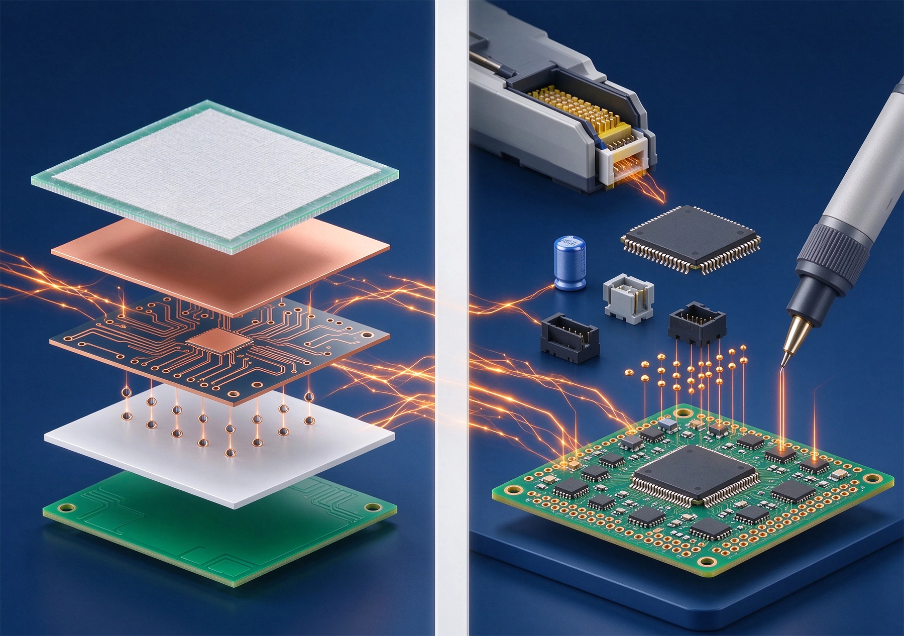
The Difference Between PCB Fabrication and PCB Manufacturing Assembly Explained

What is PCB Fabrication?

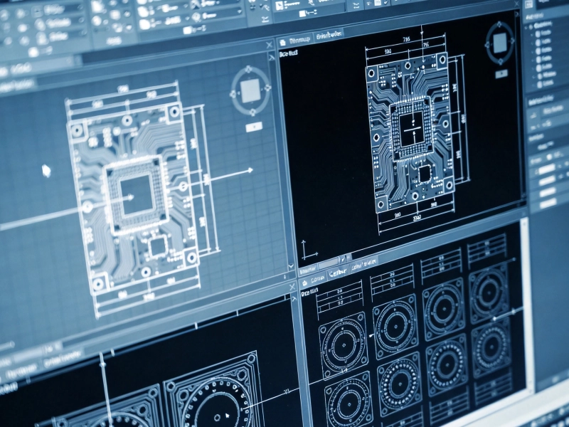
Pcb Fabrication (often shortened to "fab") is the process of manufacturing bare, unpopulated printed circuit boards from raw materials, based on your design files. The output of the fabrication process is a blank PCB with all the copper traces, pads, vias, and insulating layers as specified in your design, but no electronic components attached. Think of it like printing the blueprint for a house before you add any furniture or appliances.

Key Steps in the PCB Fabrication Process

The fabrication process typically involves 15-20 distinct steps, depending on the complexity of your board:

  1. Design file review: The fabricator reviews your Gerber Files, drill files, and fabrication specifications to check for design errors or manufacturability issues before production begins.
  2. Material preparation: Raw materials are cut to size, including copper-clad laminates (the base material for your PCB), Prepreg bonding sheets, and copper foil.
  3. Inner layer imaging and etching: For multi-layer boards, the inner layer circuits are printed onto the copper foil using Photolithography, then etched to remove unwanted copper, leaving only the desired Circuit Pattern.
  4. Lamination: The inner layers are stacked with Prepreg sheets and outer copper foil, then heated and pressed under high pressure to bond them into a single solid board.
  5. Drilling: Holes are drilled through the board for vias (connections between layers) and through-hole component pins.
  6. Plating: The drilled holes are plated with copper to create electrical connections between layers, and additional copper is added to the outer layers to build up the desired thickness.
  7. Outer layer imaging and etching: The outer layer Circuit Pattern is printed and etched, just like the inner layers.
  8. Solder Mask application: A protective Solder Mask layer is applied over the entire board, leaving only the component pads exposed. This prevents accidental solder bridges during assembly and protects the copper traces from oxidation.
  9. Silkscreen printing: Text, logos, component designators, and other markings are printed onto the solder mask layer to aid in assembly and troubleshooting.
  10. Surface finish: A protective coating is applied to the exposed copper pads to prevent oxidation and improve Solderability. Common surface finishes include Hasl (lead-free or leaded), Enig (electroless nickel immersion gold), Osp (organic Solderability preservative), and Immersion Silver.
  11. Testing and inspection: The finished bare boards undergo rigorous testing, including electrical continuity testing (usually via Flying Probe test for low volumes or bed-of-nails test for high volumes), impedance testing for high-speed boards, dimensional inspection, and visual inspection for defects.
  12. Packaging and shipping: The finished bare boards are packaged in anti-static packaging and shipped to you or your assembly partner.

What You Need to Provide for PCB Fabrication

To get your PCB fabricated, you'll need to provide:

  • Gerber Files (or ODB++ files) for all layers
  • NC drill file
  • Fabrication specification sheet including: number of layers, board thickness, copper thickness for each layer, surface finish type, solder mask color, Silkscreen color, impedance requirements (if any), and any special requirements like blind/Buried Vias, controlled dielectric, or rigid-flex construction

What is PCB Assembly (PCBA)?

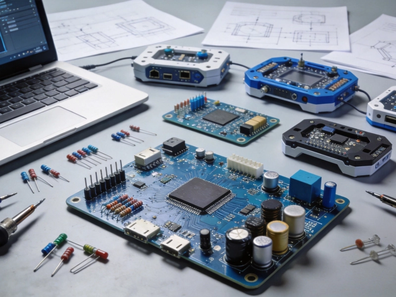
Pcb Assembly (often called PCBA, short for Printed Circuit Board Assembly) is the process of soldering electronic components onto the fabricated bare PCB to create a fully functional electronic circuit. The output of the assembly process is a completed board that can be integrated into your final product, ready to power on and perform its intended function. Continuing the house analogy, assembly is the process of adding all the furniture, appliances, and utilities to make the house livable.

Key Steps in the PCB Assembly Process

The assembly process varies slightly depending on whether you're using surface-mount (SMT) components, through-hole components, or a mix of both:

  1. Design file review and Bom Validation: The assembly partner reviews your Gerber files, bill of materials (BOM), component pick-and-place coordinates, and assembly drawings to check for issues like incorrect footprints, missing component information, or manufacturability problems.
  2. Component Procurement: The assembly team sources all the components specified in your BOM, including integrated circuits, resistors, capacitors, connectors, and any custom parts. They will verify component availability, check for counterfeit parts, and manage any long lead time components.
  3. Solder Paste printing: For SMT components, a stencil is used to print a precise layer of Solder Paste onto the component pads on the bare PCB.
  4. Pick-and-place: An automated pick-and-place machine picks up SMT components from reels or trays and places them onto their designated pads with high precision (down to 10µm accuracy for fine-pitch components).
  5. Reflow Soldering: The board with components placed passes through a reflow oven, which heats the board to a specific temperature to melt the solder paste, forming permanent electrical and mechanical connections between the components and the PCB.
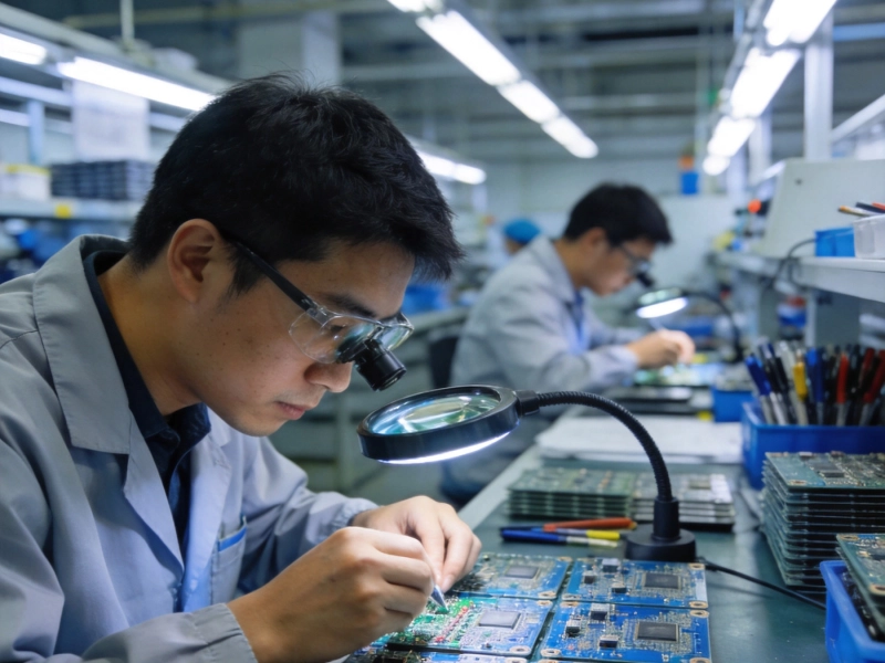
  6. Aoi Inspection: Automated Optical Inspection (Aoi) machines scan the board after reflow to check for missing components, misaligned components, solder bridges, cold joints, and other soldering defects.
  7. Through-hole component soldering: If your board has through-hole components (like large connectors, electrolytic capacitors, or power modules), these are soldered either manually or using a wave soldering machine.
  8. Cleaning: Any residual flux, solder particles, or other contaminants are removed from the board using a specialized cleaning process, which is especially important for high-voltage or high-frequency boards.
  9. Testing: The assembled board undergoes Functional Testing to ensure it works as intended. Common tests include In-Circuit Testing (Ict) to verify individual component values and connections, and Functional Circuit Testing (Fct) to simulate actual operating conditions and verify full board functionality. For high-reliability applications, boards may also undergo environmental stress testing, vibration testing, or thermal cycling.
  10. Conformal Coating (optional): For boards used in harsh environments (high humidity, dust, vibration), a protective Conformal Coating may be applied to protect the components and solder joints from damage.
  11. Packaging and shipping: The finished assembled boards are packaged in anti-static packaging, often with custom foam inserts for protection during shipping.

What You Need to Provide for PCB Assembly

To get your PCB assembled, you'll need to provide:

  • Gerber files (or the bare PCBs themselves if you're providing them)
  • Complete Bill of Materials (BOM) with part numbers, quantities, values, footprints, and approved manufacturer part numbers (AMPNs)
  • Component pick-and-place coordinate file
  • Assembly drawing with any special instructions, like component orientation requirements, press-fit parts, or testing requirements

Core Differences Between PCB Fabrication and Assembly

While both processes are part of the overall Pcb Production lifecycle, they differ significantly in almost every aspect:

AspectPcb FabricationPCB Assembly
OutputBare, unpopulated PCB with no componentsFully assembled, functional circuit board with all components soldered on
Primary ProcessesChemical etching, lamination, drilling, plating, surface treatmentSolder paste printing, pick-and-place, Reflow Soldering, inspection, testing
Required FilesGerber files, drill files, fabrication specsGerber files, BOM, pick-and-place coordinates, assembly drawing
Cost DriversNumber of layers, board complexity (blind/Buried Vias, Impedance Control), material type, surface finish, order quantityComponent cost, number of components, component complexity (fine-pitch ICs, BGA packages), testing requirements, order quantity
Typical Lead Times (low volume)2-7 business days for standard boards, up to 4 weeks for complex high-layer boards5-15 business days, depending on component lead times and assembly complexity
Quality Testing FocusElectrical continuity, trace integrity, Impedance Matching, dimensional accuracy, material conformanceSolder Joint Quality, component placement accuracy, functional performance, compliance with design specifications
Equipment RequirementsEtching lines, lamination presses, CNC drilling machines, plating linesPick-and-place machines, reflow ovens, Aoi systems, test fixtures

Common Misconceptions and Mistakes to Avoid

Misconception 1: All PCB manufacturers can do both fabrication and assembly equally well

While many companies offer turnkey PCBA services that include both fabrication and assembly, not all have equal expertise in both areas. Some manufacturers specialize in high-volume, low-complexity fabrication, while others focus on high-mix, low-volume assembly of complex boards. Always verify a supplier's specific capabilities for your particular board type before placing an order.

Misconception 2: It's always cheaper to separate fabrication and assembly

Some hardware teams try to save money by sourcing bare boards from a low-cost fabricator and then sending them to a separate assembly house. While this can sometimes save a small amount on fabrication cost, it often leads to higher overall costs due to shipping fees, additional handling, and most importantly, liability issues. If an assembled board has a problem, the fabricator may blame the assembly process and vice versa, leaving you to resolve the dispute and cover the cost of defective boards. Turnkey services from a single supplier eliminate this risk and often result in lower total cost for most projects.

Misconception 3: Fabrication quality doesn't affect assembly yield

Poor fabrication quality is one of the leading causes of assembly defects. Issues like uneven solder mask, incorrectly sized pads, out-of-spec hole sizes, or surface finish contamination can lead to solder bridges, tombstoning of components, or poor solder joints that cause assembly yields to drop significantly. Using a high-quality fabricator reduces these risks and improves overall assembly yield, saving you money in the long run.

Mistake: Asking for a "PCB price" without specifying if you need fabrication only or assembly

The cost of fabrication only is typically 10-30% of the cost of a fully assembled board, depending on the complexity of your BOM. Always specify whether you're looking for a quote for bare boards, assembled boards, or turnkey service when contacting suppliers to get accurate pricing.

Should You Use a Turnkey PCBA Service or Separate Suppliers?

The decision to use a single turnkey supplier or separate fabrication and assembly partners depends on your project requirements:

Turnkey PCBA Service (Single Supplier for Both) is Best When:

  • You're working on a low-to-medium volume project (10-10,000 units)
  • You want to minimize administrative work and have a single point of contact for all issues
  • You want clear accountability for quality issues, with no finger-pointing between suppliers
  • You need faster total lead time, as the supplier can overlap fabrication and Component Procurement
  • Your team has limited experience managing electronics supply chains

Separate Suppliers are Best When:

  • You're producing very high volumes (100,000+ units per year) and can negotiate better pricing by leveraging economies of scale with specialized suppliers
  • Your board uses extremely specialized fabrication (e.g., high-frequency RF boards, ceramic substrates, ultra-high layer count boards) that requires a specialist fabricator
  • You have an established Supply Chain and in-house quality team that can manage multiple suppliers and resolve quality disputes

For most startups, small businesses, and low-to-medium volume projects, turnkey PCBA services offer the best balance of cost, speed, and convenience, allowing you to focus on Product Development and market fit rather than managing multiple suppliers.

Summary

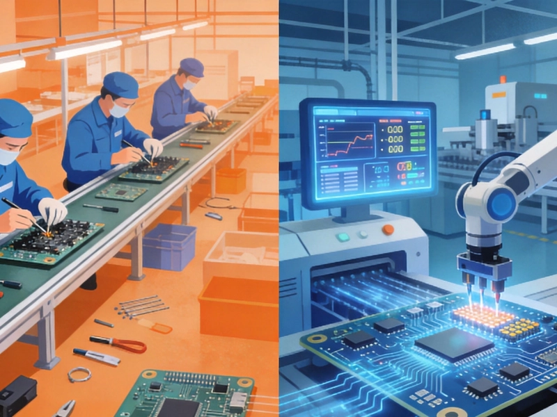
PCB fabrication is the process of making the bare circuit board, while PCB assembly is the process of soldering components onto that board to make it functional. Understanding the difference between these two processes helps you plan your product development timeline more accurately, budget appropriately, select the right suppliers, and avoid common mistakes that can delay your launch or increase costs.

Whether you need just bare PCB fabrication, full turnkey PCBA assembly, or anything in between, working with an experienced supplier who can guide you through both processes will significantly improve your chances of a successful product launch.

Contact us to discuss your requirements.
Send Message
Name*
E-mail*
Country*
Phone/WhatsApp*
Name*
E-mail*
Country*
Phone/WhatsApp*